advertisement


ALWSR Build Thread

Which user manual did you use, the latest that I successfully used is here
Which BOM did you use, I used this one here

All PCBs will lose pads on rework if you are not careful and sometimes even if you are. The hardest bit for me was fitting the pins for the wiring in the PCB, they are tight as. The PCBs are entirely adequate in my opinion.

I would agree there are some ambiguities in the documentation and BOM and areas that could be clearer, but then this is work given freely by an individual and kept alive within a community, ask for help or clarification, be patient, nobody is getting rich (or even any money!) doing this so it may make time. Hopefully you will get there and it will be worth it.
 
I've built at least 40 ALWSR's and they don't always work first time for me even now.

OK, that explains at least something...!

I noticed that the one you show in the video has no load connected. Try it with a resistive load that will sink > 5 mA which is what the Pre reg needs to operate correctly. Also I can't see the reverse of the boards to tell if you have linked TROUT to SRIN and SRGND to 0VSENSE. See figure 7 on Page 26 of the latest manual for the details.

I have these wire links. All tests done with load and without.

Don't give up. They are very much worth the trouble.

That's the part I don't understand: normally one would solder the components and if something doesn't work there is either a short, or a faulty component, or a mistake by the builder. With the ALWSRs there must be additional cases...?

First step would be a known-to-work-BOM for a safe no-risk configuration. Looking at the forum threads swapping all sorts of components to find by accident a working combination is what people seem doing to get them working.

Which user manual did you use, the latest that I successfully used is here
Which BOM did you use, I used this one here
All PCBs will lose pads on rework if you are not careful and sometimes even if you are. The hardest bit for me was fitting the pins for the wiring in the PCB, they are tight as. The PCBs are entirely adequate in my opinion.

I know these sources, went through them many times. R7 should be 1k for the LM336Z-2.5 according to data sheet...? PCBs of the new batch seem to be not of the same quality as 10y ago...? Yeah, the pins need brutal force to get into the holes. I understand nobody earns money, but it's also not a solution to let crowds of diyers each go through the same hassle of troubleshooting and trial & error...

Following on.. You could just pop them in the post to me and I could set them up for you. You've done all the boring bits and I have time to kill over Christmas thanks to COVID. You do however deserve the satisfaction of a successful result. Drop me a PM/start a "Conversation" with me here if my assistance is of interest. I enjoy a little challenge.

That is very nice of you. But I would rather like to get them to work by myself if that is possible at all. I now swapped all upper LEDs for zeners, the output voltages came closer to the desired voltages, but the flickering ones still flicker. Can faulty opamps cause flickering?
 
OK. I understand the frustration and empathise with your determination. FWIW I've never had to use force to insert any components on a new ALWSR. Might be worth soldering both sides of any component you may have had to force in as it may have damaged the through plating. Also all manual soldering is a lot easier when you don't use unleaded solder. On only one occasion have I ever had a short on any of mine and I found the solder resist to be very good, but my boards are quite elderly.

Anyway, it would help a lot if you chose one to work on first. One that is stable/steady state would be good. You need to feed it with approx 4 volts more than the desired output voltage. If you could then draw the schematic or print off the one from the manual and annotate it with any changed component values and the voltages at each junction and post the resulting schematic, along with a photo of both sides of that same board that would be a great help. I know it is laborious but it is the only way we can help you find this.

John
 
Upon further examination I can just about make out that at least some of the ZTX transistors are the wrong way round. The curved face of the cases of both of these transistors should face towards the bottom left of the boards, i.e. towards the input terminals. I'd be lying if I said that i have never done this myself. To remove them you are best off flooding their pins on the reverse of the board with solder so you can heat them all at the same time. A solder sucker will likely then be needed to remove the excess and clear the holes.

Edit: Have zoomed in and T1 and T2 are rotated 180 degrees on every board. Collector is pin 3 on these.

Everything else looks perfect.

John
 
I checked the 317 on the flickering board again and replaced it the second time, now it shows correct voltage but the LED still flickeres. Here the components I used:

- C1, C4, C_Kelvin = 47u NHG
- C2 = 100u OSCON
- C3 = 22u NHG
- C5, C6, C7 no fit
- D2 = 1N5333B
- R5 = 2k5
- R7 = 1k
- ZD1 = LM336Z-2.5

all other parts as in manual PDF v2.9-rev009

T1 and T2 are rotated 180 degrees on every board. Collector is pin 3 on these.

I have them the wrong way round?!?!? The manual PDF shows the ZTX as "C-B-E"...
 
I know these sources, went through them many times. R7 should be 1k for the LM336Z-2.5 according to data sheet...? PCBs of the new batch seem to be not of the same quality as 10y ago...? Yeah, the pins need brutal force to get into the holes. I understand nobody earns money, but it's also not a solution to let crowds of diyers each go through the same hassle of troubleshooting and trial & error...

I tried to document the issues I found. I have had much more grief from worse document commercial products. Feel free, once you have them working, to improve on the documentation for those that follow?
 
Good idea. We should summarize an addendum for the manual which covers all issues.

Even better would be to design a new board, same circuit/layout, but correct hole sizes, silk screen, actual BOM etc. etc.
 
Last edited:
Plus have a go at a lower voltage version for dacs etc and a higher voltage one for power amp front ends. Oh and an optional VBE before the pre-reg for when you have the voltage headroom. ;)
 
My thoughts:

Rather than change the PCB, and as far as I know the only real issue I had was the wire pins were too tight a fit to be comfortable, could an alternative pin that isn't so tight be specified? It is less the PCB is wrong, more the pins suggested on the BOM are wrong? There is a good reason for this: layout is critical to stability I believe, components are tight fit to ensure minimum component leg reducing the potential for parasitic effects and resulting instability.

Silkscreen adds cost, which is presumably why it was not done, this isn't a real problem if provided separately, as the manual does, *if* it matches the BOM and is up to date and it covers all variants ...

Having one BOM for multiple variants is part of the confusion in my opinion. One BOM per variant would be better, and by variant I mean each build, so a +5V, a -5V, a +not 5V and a -not 5V, perhaps with pre-reg, without pre-reg on each of those, and Tim's VBE for higher voltage versions ... all good but all worth a separate BOM and a separate component overlay perhaps? More work, harder to maintain, but less confusion for a first time builder.

Photos of working versions help, if you have a well taken photo to copy it is harder to go wrong.
 
OK, if I do it we need the exact info for the high voltage version and also for the VBE!
I was being a bit tongue in cheek with my suggestions. This is the intellectual property of Andy Weekes after all
 
Of course I wouldn't proceed if Andrew does not agree. I would keep the layout but make it easier to work with. For example with the TO220s at the short side of the board. Configuration I usually do with solderjumpers. Low current parts could be large SMDs, PCB could be even smaller. All pins could be in one row so it would be possible to plug them into a main board like the cards in the NAC72. BOM could cover all variants in one Excel sheet. It would be like a refined version of the original.
 
Last edited:
I was being a bit tongue in cheek with my suggestions. This is the intellectual property of Andy Weekes after all

Only the PCB design, almost all of the background work and design is attributable to Walt Jung and these were built on those giants shoulders.

I'm sorry some have struggled with these, you have to bear in mind the PCB design is pretty old now and because I had to drop away from being involved regularly with the project after years of satisfying, but time-consuming involvement, the parts lists and availability has changed quite a bit in that time.

I'd certainly do this differently were I to re-visit it, maybe one day that will happen! Certainly a little more spacing for component size variations would be on the list and I'd have a silk screen, the cost of adding one isn't that significant.

The bootstrapped nature of the design does make troubleshooting hard, but when built correctly they are remarkably tolerant of component variations, most issues come down to build errors or the occasional PCB short. The full schematics are available so it's pretty easy to check any component substitutions are fitted correctly.

Given the thousands out there in regular use and still working decades later, there's clearly nothing fundamentally wrong with the design, but I haven't kept it up to date as obsolescence has happened, for that the community has had to fend for itself. I only sell boards to satisfy demand now, the two recent batches being the first I've ordered since 2011, and even back then they were for a reseller, to save me the time to organise deliveries.

Maybe I should have made the above clearer, but the recent batches have been solely to satisfy the constant demand I still receive (which is both astonishing and flattering!) not because of any great profit motive on my part.

As the design is fundamentally built on Walt's work, anyone is free to take that and work with it and give that attribution, my contribution is/was largely in the PCB design and I'm not precious over it. It is a good layout, from a fundamental electrical perspective, but it could certainly be better from a practical perspective.

Most of the alternative PCB designs I've seen over the years have failed to understand the concept of the PCB as part of the electrical circuit and failed to address the errors that can arise as a result, but I'm not the only person capable of doing a good PCB design!
 
  • Like
Reactions: jpk
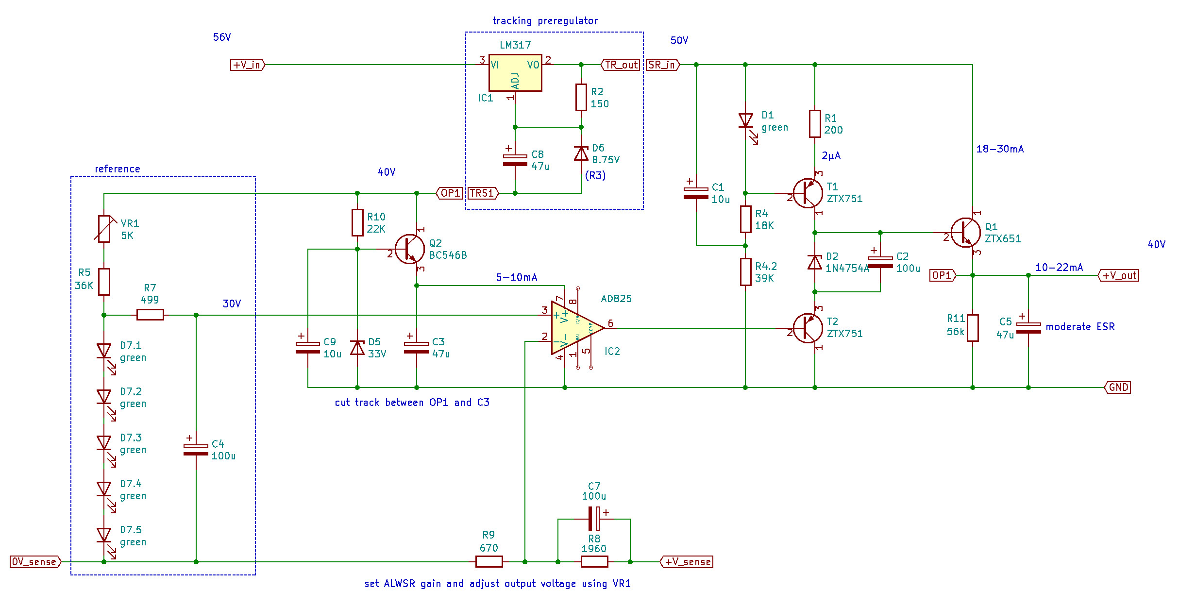
OK, I put together a schematic, inspired from here, for a 40V version as a drop in replacement for the regulator board in Naim style power amps to power the front end (when running the power stage from a raw PSU):

iOfbMDi.jpeg


Here is the negative version. I am not sure about the voltage in the LED string and also how to adjust the pre-regulator.

Oh well at least it took up a bit of lockdown time

timH, did you manage to build your high voltage version?
 
Last edited:
Well wouldn’t you know I just started it this morning. :)
Currently struggling with soldering together 7 x smd green leds for the voltage ref

:cool: Oh, cool! Would you be so kind and let me know if there are errors in my schematic...?
 
I’ve had a quick look and it looks fine. It’s key where you cut the track from OP1. It needs to be between OP1 and C3+ rather than between C3+ and Opamp pin 7. of course these comments depend entirely on whether mine actually works :)
Also I’ve made a couple of cuts to tracks between C1 R4 and 0v pwr. If it all works I’ll post some pics


advertisement


Back
Top