advertisement


Best CD clock upgrade?

I wish I could add something here other than encouragement and the fact that Eagle will handle the earth plane...

This could turn into a standard mod ;)
 
Ok, here's my next try. 0v returns have been kept short where they matter most, hopefully this is much better, albeit without a ground plane.

XO-psu-PCB3.png
 
Andrew L Weekes said:
But not as low as Martin's circuit, at the real frequencies of interest.


Therein lies the answer - think phase noise, think spectra, think what's most important in terms of jitter and it's audibility ;)

Andy,

You know more than me here - tell me what you think!

My argument is that noise is not the issue - a "crap sounding" 3 pin reg followed by a cap multiplier will be quieter than a reg on its own. The cap multiplier wqill lower noise and increase output impedance at low frequencies.

But I can't see how low output impedance at audio frequencies will have any relevance because, as you say, it's the cap next to the XO that matters at several MHz.

I'm happy to accept Martin's experience of crapness with the Tent style supply, but much of the fun of audio - to me anyway - is trying to correlate what we hear and measure with an understanding of what's actually going on

Dan
 
Carl,

Here's some food for thought...

XO_PSU.gif


Shorter ground paths and a tighter layout (could probably tighten it up a little further with more work, but it's not bad for a first iteration!), you could add the clock to it quite easily, maybe just shift a few things around at the RHS.

Of course, surface mount is the way to go here ;)

Anyway it's fun doing PCB layout, it appeals to the artistic element in me, but since I can't draw for toffee, the 'rules' element of it allows me to do something a bit artistic, within electrical constraints. It's quite relaxing really...

Andy.

P.S. You need a ceramic / film bypass cap across the XO module's PSU pins, with the shortest possible traces between the pins.
 
Here's the idea using a ground plane (which Eagle would handle, Carl, if you fancy trying it). I've included the XO on this too.

XO_PSU2_1.gif


With copper area showing

XO_PSU2_2.gif


Copper area removed to show traces
 
Now that's much better!

All it needs is a couple of pin-holes for the 33R / 100R outputs to DAC / decoder and it's the business. Can you send me the Eagle files please Andy? I'll have a bash with it and see what's what. [email protected] (remove YOURHAT for it to work ;) )
 
Carl,

I'm sorry but that wasn't done in Eagle :(

At least you can lay it out in Eagle and not have to worry about the physical bits, just the operation ;)

Andy.
 
Andy,
In your PCB design lesson it looks as though the ground plane replaces the 0v traces, I'm not sure if I understand this correctly.
Ashley
 
In your PCB design lesson it looks as though the ground plane replaces the 0v traces, I'm not sure if I understand this correctly.

That's correct.

It's a technique that's often essential at RF frequencies - the large mass of the copper ground plane area provides several advantages: -

1. Lower impedance. A long (electrically) trace at RF won't look like a short to ground (it might, depending upon length), it could look inductive, capacitive or like an open circuit, if the trace has significant length compared to the wavelength of the frequency of operation.

2. Allows the use of traces as circuit elements (stripline) - you can design traces to have specific impedances, impedance transformation properties t behave as inductors etc.

The thing with audio is you want to know where the currents are flowing and you also have to watch for capacitance (the traces on the bottom layer will exhibit additional capacitance, based upon their area, the thickness of the PCB and it's dielectric properties.

In a board such as this, the return current flow will follow the +ve feed current, so you have to be careful that a large current (or more properly significant relative to the signal levels / impedances in the circuit) doesn't flow across an area where there's a sensitive area of circuitry, giving rise to errors, noise and other artifacts.

The advantage in this instance is we've placed a high-frequency source (the clock) on the same board as an op-amp with 130dB of open loop gain and absolutely tiny error signals at it's input pins. The ground plane provides a low impedance ground path for an HF signals flowing within the circuit, and I've positioned the ground points in order to try and prevent the return currents from individual ground points crossing sensitive circuitry and giving rise to errors, or worse, instability.

The trace capacitance is less of an issue here, since most of the impedances are low, and where they aren't, the capacitance to ground is most likely beneficial, not degrading.

One has to look at PCB design in this way - copper is not a superconductor, traces have capacitance, inductance and resistance and you have to consider their effect on your circuit.

I always think of circuit traces as having significant impedance in my head, when laying out a board, that way you can consider their effect on a circuit's performance - 1mA flowing through 1mOhm is 1uV, which is in the order of the voltages present at the AD797 op-amp's input!

Andy.
 
Andy,

That explanation is testament to why it's a good job that you rejigged the circuit instead of leaving it to me. Marvelous stuff.

I take it in this layout that the 0v pin is shared; in other words, it is the 0v point for the +ve supply and the 0v return for the clock output?

I'm guessing that your s/w can export all the gerber files, drill templates etc necessary for a pcb company to knock up a few of these boards? If you get time, can you add two pin-holes linked to the 33R and 100R? That would allow easy connection of miniature coax and we can then think about getting some costs for production nailed down.

I don't mind organising things... does anyone have any recommendations for a company that can do cheap production of small quantities of pcbs?
 
I take it in this layout that the 0v pin is shared; in other words, it is the 0v point for the +ve supply and the 0v return for the clock output?

Err no, that's what we call, in the engineering parlance, an oversight (or cock up!) :)

Well spotted...

Andy.
 
Andy,

Thanks for that detailed response, I think I'm starting to understand a little. However there is one point I can't get my head around and that is
In a board such as this, the return current flow will follow the +ve feed current
So for instance looking at the opamp pin 7 connection to the ground plane will the current flow directly to the 0v star point or will it follow the opamp supply trace upto the 0R5 resistor and then flow to the 0v star point.

I do notice that you have put almost all your ground plane connections below the sensitive opamp so that direct paths would not flow near the sensitive opamp.
Ashley
 
So for instance looking at the opamp pin 7 connection to the ground plane will the current flow directly to the 0v star point or will it follow the opamp supply trace upto the 0R5 resistor and then flow to the 0v star point.

Good question!

It's worth talking about this a bit more, especially as you have to think about the frequency components of the power too - as we all know by now, it's not just DC current flowing, but an element of AC too. The AC component comes from several sources, e.g. noise on the incoming supply, current variations in the circuits being powered etc. Herein lies the biggest clues as to how to solve the potential problems that arise.

If we were to remove all the local bypass and decoupling caps, the current path in the ground plane would run under all of the traces associated with the current flow into the circuit, i.e. the flow in the ground plane would follow the path of least inductance, which is always going to be the point at which the traces have the smallest physical seperation.

This results in a large 'loop' area which gives rise to both noise sensitivity and noise emissions problems. The key thing to realise is that all the current is flowing in that path, the DC and the higher-frequency components.

The HF components are the largest problem, the impedance of the ground paths at DC are easy to determine, they are simply the resistance of the copper traces or the plane area (very low, in a plane). As frequencies rise though, the reactive parts of the circuit become dominant - if the ground path looks inductive you now have problems with voltages at that point not being what you expect as the current flow in them gives rise to errors. The worst problems are the circuit elements can become resonant, as their inductance rises and stray capacitance dominates, giving rise to massive increases in voltage levels and radiated noise, or becoming high impedance and now being sensitive to EMI surrounding the circuit.

The key then is good decoupling. By adding local bypass capacitors we 'short circuit' the high frequency components on the rails to ground and provide a local reservoir of energy storage to deal with peaks in demand. If we do this properly, and ensure the loop areas formed by these decoupling components are as small as is practically possible, the radiation drops dramatically.

We're left with only the low frequency and DC components flowing in the secondary return path (which is the large loop area) and these are relatively trivial to deal with (but should not be overlooked in precision applications). The things to then look out for are 'high' currents flowing across the ground point for a critical circuit element, for example, giving rise to a DC or LF error as the ground potential at that point changes (through simple Ohms law). Remember all voltages have to be measured relative to something. If one part of a circuit measures it's voltage relative to a 'ground' that's at a different potential to another part of the circuit, you can give rise to an error that's equal to the potential difference between the points.

Now you know why the star point / single point earthing is so critical in precision measurement systems (which is what audio is!).

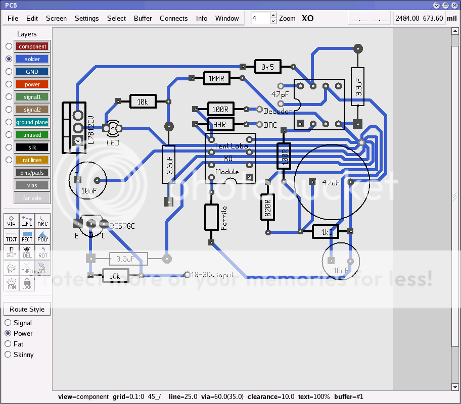
Another technique to further enhance this effect is to add some additional impedance in the PSU feed, this can be a resistor (Naim's 27R / 47u combo for example) or an inductor or some combination. You have to be careful though in different circumstances - ferrite-based inductors exhibit non-linearities that can sometimes be audible, air-cored indctors exhibit high Q and can form lovely resonant circuits with the high-Q decoupling caps. In this case we've added a 0.5R in series with the op-amp feed, this enhances the effect of the 3.3u cap and also means the 7812 doesn't see a high-Q circuit shorting it's ouptut at HF, which might give rise to oscillation or quasi stability in the regulator.

At the input to the 7812 we have another cap, this acts in conjunction with the cap multiplier to further filter any incoming noise, so there's a current 'loop' here too (i.e. input pin, cap multiplier, 10u back to ground.

So this apparently simple circuit has had quite a lot done to it, to keep HF noise currents out of the circuit and well controlled - the only thing I think that might be worth adding to it is an input bypass cap, right at the power input to the board.

Andy.
 
Andy,
Thanks very much for the excellent teach in, I'll go and have a play!
Ashley


Hacker,
Don't know if this link to a PCB manufacturer on ebay is worth checking out.
 
This site contains affiliate links for which pink fish media may be compensated.
I'll try and finish the board today, then someone can check it for errors (it should be right, as it's produced from a schematic netlist).

Once happy I'll run Gerbers and we can get some quotes.

Please confirm dimensions of the XO too - Guido's site doesn't have an outline dimension AFAICT, but I've based it on a 'standard' part.

I also want to reduce the size of the decoupling cap on the clock to make it less inductive - anyone have a problem with SMD here, it's by far the optimal solution and I strongly recommend it?

Andy.
 
Andy, thanks again for the detailed info - much to digest there.

The XO is a standard DIL8 package size, although it only has 4 pins (one in each corner, pins 1,4,5 and 8 of a DIL8).

SMD is fine for me... I guess we'll just need steady hands for soldering!

Carl.
 
OK, I've almost finished - the decoupling for the clock module only is now SMD as are the two output resistors (33R / 100R).

A question for all involved (including Martin) I was going to mark the 'design' as copyright PFM, and in effect donate it to the site, free for anyone to use *for personal use only*.

Anyone with commercial intentions would then have to sort out an agreement with Tony L.

Is that acceptable to everyone?

Andy.
 
Acceptable? I hope I speak for all us DiY-ers when I say that it's incredibly generous of you and Martin to donate your knowledge, effort and time like this.

I think I'm gonna play with old PCBs now to get a decent SMD soldering technique... ;)
 
Andy , two quickies - yes, add a decoupling cap to the raw input if you haven't already, anything over 1uF is good and helps keeps any rectifier noise out of the rest of the circuit - and circuit ground.

Secondly - definitely copyright this one PFM (Pink Flea Modulator?). Share and enjoy!


advertisement


Back
Top