davidsrsb
pfm Member
Japanese numbers are a real pain as they are never reused by a second source, like the US and European numbers.
I try to suggest parts in RS. Cricklewood are also trustworthy, but never buy from eBay.
I have not found a datasheet for the 2SC632
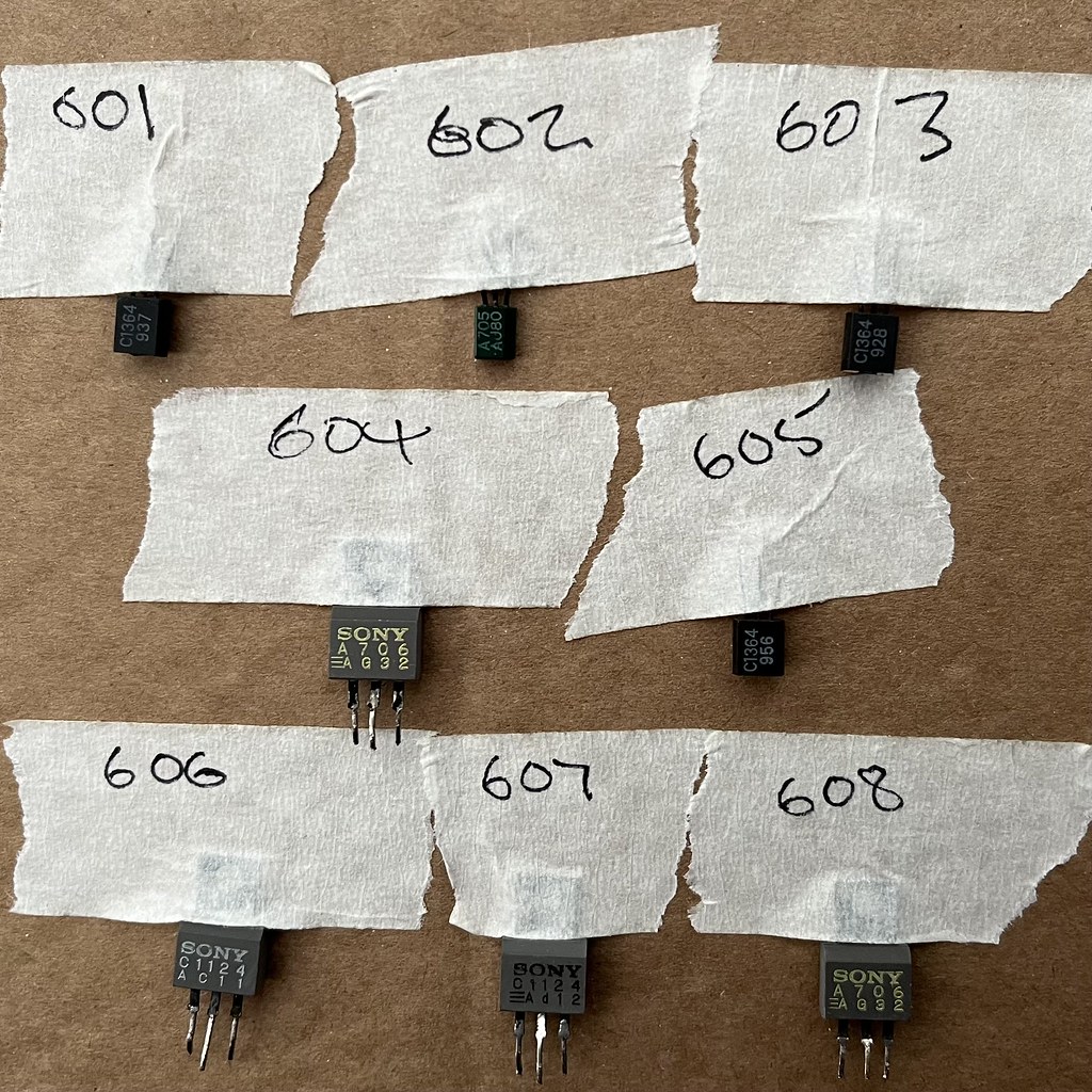
Please examine you actual PCB very carefully and give us the actual part numbers, there are variations between closely related models.
The 2SC632 and 2SC632A are not exactly the same. Swapping parts with better noise or higher voltage is fine. Too high or low gain can be an issue and too fast can turn a very poor PCB layout into an oscillator.
I try to suggest parts in RS. Cricklewood are also trustworthy, but never buy from eBay.
I have not found a datasheet for the 2SC632
Please examine you actual PCB very carefully and give us the actual part numbers, there are variations between closely related models.
The 2SC632 and 2SC632A are not exactly the same. Swapping parts with better noise or higher voltage is fine. Too high or low gain can be an issue and too fast can turn a very poor PCB layout into an oscillator.