advertisement


Sony 7ch receiver gone DC

a.palfreyman

pfm Member
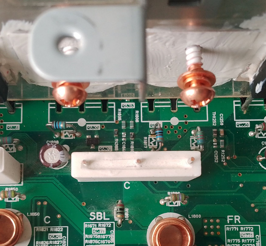
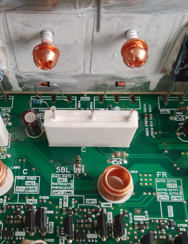
Looking at a Sony STR-DN1080 for a friend as it keeps going into 'Protector' mode. After much head scratching (plus a bit cursing) I eventually traced it to the centre channel OP transistors having gone west...
Would like to try to measure the associated current detect, limiter and poweramp transistors, but the are all smd...and will be a PITA to check.
DIYA member 'jkuetemann' reckons that most failures occur as a straight failure of the OP transistors after getting thrashed as they are never fitted tightly enough to the H/sink. The emitter resistor pair measures OK.
Any thoughts?
There's an ebay listing for s/h OP transistors taken from a Sony unit so was going to go down that path.
 
Not my amp. Date code inside is 09/17. He also admitted to doing something naughty, but I don't know the full details.
Anyway, pair of new 100R resistors fitted (which go to the bases of the OP pair) as one was up to 111R, other was O/C:
IMG-20240326-082920-921-2.jpg

Other than that, everything else around the OP stage seems to compare with the adjacent stage. Awaiting a pair of transistors now.
 
Didn't want to risk blowing it up if I'd missed something so replaced the OP devices B>E positions with diodes, reconnecting the feedback loop. Quickly reinstalled and tested and all good, as the DC offset was nice and low.
IMG-20240329-124635-883-2.jpg

Put the OP devices in, but there isn't quite enough thermal paste on the new devices, and the rest is a bit of a mess, so going the remove the h/sink and redo the lot.
 
Yes, seems to work though. I suspect the 100R base resistors blowing saved the rest of the circuit/circuit board....it was lucky I had some similar sized ones in my spares box.
 
Removed the H/sink and the mica insulators, cleaned it up and replaced with new ones and fresh Kontakt Chemie paste. Biases up OK with low DC offset on all channels. Measures from 4.2 to 4.7mV bias across each pair of 0R22 emitter resistors. Ran the repaired centre channel for about 20 mins, building up from a low value up to 2W. All good. :)
 
On the output devices, collectors go to the supply rails and bases are fed with a bias voltage of about 2.1V between them. So, you put have:
100R>npn BE>0R22>0R22>pnp BE>100R. Centre of 0R22 goes to FB network. If something was awry, there was a possibility that I'd have just blown the new transistors, so I substituted each of the BE junctions with a diode facing appropriate to the BE junction. This reconnects the FB network with an appropriate voltage drop either side giving a bias current of about 4mA as it's 2.1v - 1.3v (2 diodes) gives 0.8v. 0.8/200R is 4mA. That's ample to make sure other parts (such as transistors that drive the outputs or fix the bias voltage etc) are working appropriately.


advertisement


Back
Top