
You are using an out of date browser. It may not display this or other websites correctly.
You should upgrade or use an alternative browser.
You should upgrade or use an alternative browser.
555PS DR Towering Inferno – Resistor Values Needed Please
- Thread starter Cloth Ears
- Start date
Schematic, taken from XPS schematic and modified according to the information in this thread:
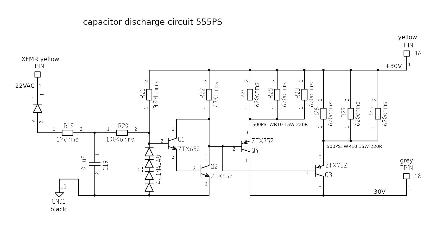
The supply to the input labelled "22VAC" comes from the minus leg of one of the bridge rectifiers in other PSUs such as XPS and TPRX. Since the 555 uses TO220 diodes instead of the bridge rectifiers there is an additional diode, drawn as a Zener in the first post of this thread...
The supply to the input labelled "22VAC" comes from the minus leg of one of the bridge rectifiers in other PSUs such as XPS and TPRX. Since the 555 uses TO220 diodes instead of the bridge rectifiers there is an additional diode, drawn as a Zener in the first post of this thread...
rontoolsie
pfm Member
Here is the complete schematic for the original 555PS. The resistor values you are interested in are probably identical
https://www.dropbox.com/sh/fnp1nami9iguwjj/AACIN1LaDmuLCS6ywjWLaKipa?dl=0
https://www.dropbox.com/sh/fnp1nami9iguwjj/AACIN1LaDmuLCS6ywjWLaKipa?dl=0
Cloth Ears
pfm Member
Hi Guys,
Firstly an apology to those who have been helping me or read this thread and wondered how the story ends. Unfortunately I had to put this to one side for the last couple of months due to other unavoidable commitments but I’m back on the case now.
Thanks to JPK for providing the Naim schematic of the 500PS discharge circuit modified to incorporate the values supplied by hp1. It compares favorably with my reverse engineered sketch.
JPK I can confirm the diode which senses the 22V AC transformer supply is not a Zenner as drawn in the sketch on the first post. I think it reads RL03 (which I cannot find) but looks like a fast recovery diode. I have some of these to try.
Thanks also to Rontoolsie for posting the complete original 555PS Schematics unfortunately I can only see the regulator circuits but I think I now have enough information to start repairing and experimenting.
The plan is to first determine if my unit had been fitted with incorrect resistors during manufacture by severely overloading several SFR25 620R resistors and see what happens to the resistance value i.e. does it drop to around 68R like my burnt ones.
Then I will build a couple of these discharge circuits to verify the operating parameters and determine exactly how much energy is dissipated during discharge under normal operation. I would also like to fail each component in the circuit to see how it performs from a safety point of view – cue my thermal cutout and chunky resistors.
I’ve never used Spice circuit simulation until now but thought it would be interesting to try simulating the circuit before I started on real life fireworks.
For a basic circuit like this I found LTSpice quite easy to use (apart from constructing a transformer from inductors) and it has provided some really useful information so far.
My original description of how I thought the circuit worked was, for the most part, correct. However, I did not appreciate that when the discharge takes place transistors TR1 and TR4 (Q3,Q4 in the Naim scheme) are not turned hard on placing the full 60V (+30,-30) across the discharge resistors. At the first instant of discharge the Collector- Emitter voltage on these transistors is around 32V leaving the voltage across the six discharge resistors of 28V.
As the voltage on the +30 -30 rails falls so does the Collector- Emitter voltage and subsequently the voltage across the discharge resistors.
This discovery immediately more than halves the initial value of the discharge current flowing through the six 620R resistors. From what I thought was 60/620 = 0.097A = 5.8W per resistor to 28/620 = 0.045A = 1.26W per resistor – much more acceptable on a 0.4W resistor.
Here is a picture of the LTSpice simulation circuit I used:-
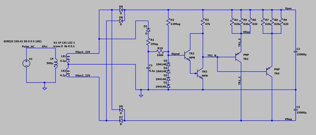
As a first time user I found the LTSpice to be excellent and it was just like being at the workbench with an unlimited supply of parts and a magic soldering iron. It’s so easy to put a circuit together, connect it to a power supply and see it work…..or not.
Just a few notes on the circuit above for those not familiar with LTSpice.
V1 is an AC power supply configured to generate a mains voltage at 50Hz for 2 seconds before it stops. This represents turning the amp on and allowing the 15,000uF caps to charge before it switches off and the discharge takes place.
Its output voltage is set to 339.41V as this is the peak to peak voltage representing 240V RMS (just ignoring all that fictitious 230V for now).
The transformer is ratioed at 10.9 to 1 by the choice of inductor values in Henries. This gives 240v RMS in and 22V-0-22V RMS out – just like in the real 555PS.
The statement beginning K1 tells Spice the three inductors are a transformer for 8 seconds.
The rest is fairly self explanatory. When you hit run the 22V secondaries are on for 2 seconds then the discharge circuit cuts in and the +30 -30 V rails both converge towards OV over the next 6 seconds. A graph window pops up and it is possible to observe just about every voltage and current depending on what is selected.
I will see if I can post a copy of the actual spice file and some very interesting graphs.
Firstly an apology to those who have been helping me or read this thread and wondered how the story ends. Unfortunately I had to put this to one side for the last couple of months due to other unavoidable commitments but I’m back on the case now.
Thanks to JPK for providing the Naim schematic of the 500PS discharge circuit modified to incorporate the values supplied by hp1. It compares favorably with my reverse engineered sketch.
JPK I can confirm the diode which senses the 22V AC transformer supply is not a Zenner as drawn in the sketch on the first post. I think it reads RL03 (which I cannot find) but looks like a fast recovery diode. I have some of these to try.
Thanks also to Rontoolsie for posting the complete original 555PS Schematics unfortunately I can only see the regulator circuits but I think I now have enough information to start repairing and experimenting.
The plan is to first determine if my unit had been fitted with incorrect resistors during manufacture by severely overloading several SFR25 620R resistors and see what happens to the resistance value i.e. does it drop to around 68R like my burnt ones.
Then I will build a couple of these discharge circuits to verify the operating parameters and determine exactly how much energy is dissipated during discharge under normal operation. I would also like to fail each component in the circuit to see how it performs from a safety point of view – cue my thermal cutout and chunky resistors.
I’ve never used Spice circuit simulation until now but thought it would be interesting to try simulating the circuit before I started on real life fireworks.
For a basic circuit like this I found LTSpice quite easy to use (apart from constructing a transformer from inductors) and it has provided some really useful information so far.
My original description of how I thought the circuit worked was, for the most part, correct. However, I did not appreciate that when the discharge takes place transistors TR1 and TR4 (Q3,Q4 in the Naim scheme) are not turned hard on placing the full 60V (+30,-30) across the discharge resistors. At the first instant of discharge the Collector- Emitter voltage on these transistors is around 32V leaving the voltage across the six discharge resistors of 28V.
As the voltage on the +30 -30 rails falls so does the Collector- Emitter voltage and subsequently the voltage across the discharge resistors.
This discovery immediately more than halves the initial value of the discharge current flowing through the six 620R resistors. From what I thought was 60/620 = 0.097A = 5.8W per resistor to 28/620 = 0.045A = 1.26W per resistor – much more acceptable on a 0.4W resistor.
Here is a picture of the LTSpice simulation circuit I used:-
As a first time user I found the LTSpice to be excellent and it was just like being at the workbench with an unlimited supply of parts and a magic soldering iron. It’s so easy to put a circuit together, connect it to a power supply and see it work…..or not.
Just a few notes on the circuit above for those not familiar with LTSpice.
V1 is an AC power supply configured to generate a mains voltage at 50Hz for 2 seconds before it stops. This represents turning the amp on and allowing the 15,000uF caps to charge before it switches off and the discharge takes place.
Its output voltage is set to 339.41V as this is the peak to peak voltage representing 240V RMS (just ignoring all that fictitious 230V for now).
The transformer is ratioed at 10.9 to 1 by the choice of inductor values in Henries. This gives 240v RMS in and 22V-0-22V RMS out – just like in the real 555PS.
The statement beginning K1 tells Spice the three inductors are a transformer for 8 seconds.
The rest is fairly self explanatory. When you hit run the 22V secondaries are on for 2 seconds then the discharge circuit cuts in and the +30 -30 V rails both converge towards OV over the next 6 seconds. A graph window pops up and it is possible to observe just about every voltage and current depending on what is selected.
I will see if I can post a copy of the actual spice file and some very interesting graphs.
Great!!! When I saw the original schematic Ron has posted I was impressed to find the exact same basic LM317 circuits as in the XPS2, and I wonder how the 555PS can sound so much better than the XPS2, plus the 555PS seems to be really expensive for what it is in regard to the circuits it contains...
Cloth Ears
pfm Member
Not sure if this is how to post a link to a file but this should be the operational file for the LTSpice schematic shown above.
To view it and run it you will need to download and install the free LTSpice program from Analog Devices.com - well worth having.
https://www.dropbox.com/s/0tli5j7idvwgbga/555PS Discharge Circuit 1.asc?dl=0
When Dropbox opens click continue to website then click the download icon next to the sign up button.
Is there a better way of doing this - seems a bit convoluted ?
Last edited:
Cloth Ears
pfm Member
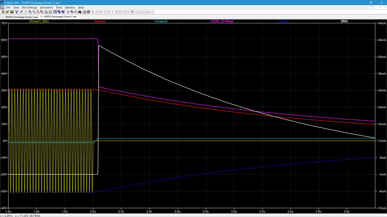
Here are three graphs captured from the Spice simulation of the 555PS discharge circuit. It is possible to graph any of the voltages and currents in the simulation but it soon becomes very cluttered if you put it all on together. The simulation captures 8 seconds of data – 2 seconds with the transformer charging the caps then 6 seconds with the caps discharging via the resistors. I have ran it up to 100 seconds but there are always just a few volts on the caps once the discharge circuit cuts out. If I added the residual load of the regulators this would fall quicker and more completely towards 0V.
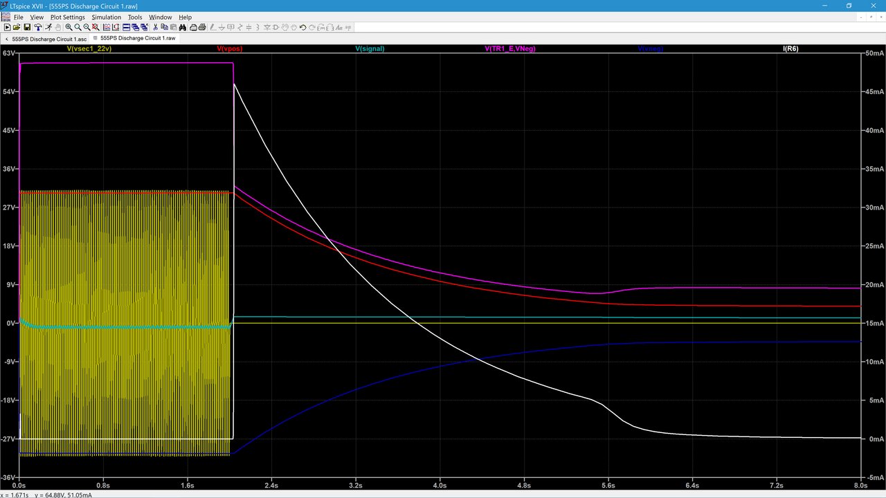
The first graph above shows the full 8 seconds and gives an overall view of the switch on, switch off and discharge. Notice that the timescale is horizontal along the bottom, the AC and DC voltages are at the left side and the current scale is on the right side. The colours of the traces are the same as the trace names at the top and here is a short description of each one and what is happening:-
V(vsec1_22v) Yellow
This is one phase of the 22V transformer secondary (other phase still operating but omitted for clarity) which runs for 100 cycles – 2 Secs before going to 0V
V(vpos) Red
The rectified +30V DC voltage feeding the regulators. Notice how it drops down towards 0V as soon as the discharge circuit cuts in. By 7.4 sec it has reduced to 8.2 volts and by that point the discharge current is practically 0mA. I ran this for 100 secs and went down to about 4V but there was no regulator load added to make it go to 0V.
V(Signal) Pale Blue/Teal
This is the control signal derived from the 22V transformer winding via diode D1and resistor R1 and smoothed by C1. It is trimmed via the 4 IN4148 diodes and when the transformer is live produces a -1V hold off signal to the Darlington pair TR2/TR3 which biases the discharge transistors TR1/TR2 off until the transformer output ceases. When the 22v AC goes off the signal rises to just above 1V positive and initiates the discharge.
V(TR1_E,VNeg) Magenta
This is the emitter/collector voltage across the transistors which actually switch the discharge resistors into circuit. They start at the top left with the full 60V across them from both 30V supply rails. However, they don’t just switch fully on but control their voltage to 32 at the start of discharge then fall as the supply rails fall. Remember the voltage scale is on the left for all voltages.
V(VNeg) Dark Blue
This is the negative supply rail and can be seen rising from -30V towards 0V from the start of the discharge.
I(R6) White
This is the all important discharge current and can be seen at the start passing a small blip of current until the control signal establishes a -1V signal. It remains at 0mA until the transformer goes off and the control signal rises to just over 1V positive. The discharge current quickly peaks at around 45.9mA (per resistor) until it gradually comes back down to 0mA at around 7.4 Secs.
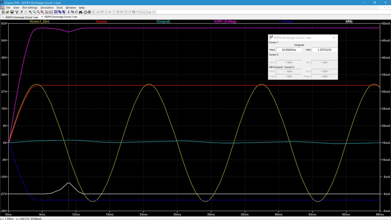
The graph above shows a zoomed in section at the very start of switch on. Note that at 10mS the control signal is at 1.35 positive which causes a momentary triggering of the discharge circuit with TR1/TR2 beginning to conduct and a 5mA pulse of current through R6 (and the other 5 discharge resistors) until the signal becomes -1V at the next cycle.
mmmm... I know that one is at start up but I wonder how many other times it goes into discharge mode whilst on. I will look out for that when I get a real scope on the real experimental circuit. Going into discharge mode whilst powered on may be the start of my Towering Inferno.
This graph above shows a zoomed in section from 1.4 sec after switch on and shows very clearly the operation of the control signal as it crosses from minus 1V to plus 1 to 1.5V at the end of the 2 second period where it initiates the discharge.
Apologies for the quality of the images they look great on my PC
Edited - Images reloaded with trace width increased - looks a bit better.
The first graph above shows the full 8 seconds and gives an overall view of the switch on, switch off and discharge. Notice that the timescale is horizontal along the bottom, the AC and DC voltages are at the left side and the current scale is on the right side. The colours of the traces are the same as the trace names at the top and here is a short description of each one and what is happening:-
V(vsec1_22v) Yellow
This is one phase of the 22V transformer secondary (other phase still operating but omitted for clarity) which runs for 100 cycles – 2 Secs before going to 0V
V(vpos) Red
The rectified +30V DC voltage feeding the regulators. Notice how it drops down towards 0V as soon as the discharge circuit cuts in. By 7.4 sec it has reduced to 8.2 volts and by that point the discharge current is practically 0mA. I ran this for 100 secs and went down to about 4V but there was no regulator load added to make it go to 0V.
V(Signal) Pale Blue/Teal
This is the control signal derived from the 22V transformer winding via diode D1and resistor R1 and smoothed by C1. It is trimmed via the 4 IN4148 diodes and when the transformer is live produces a -1V hold off signal to the Darlington pair TR2/TR3 which biases the discharge transistors TR1/TR2 off until the transformer output ceases. When the 22v AC goes off the signal rises to just above 1V positive and initiates the discharge.
V(TR1_E,VNeg) Magenta
This is the emitter/collector voltage across the transistors which actually switch the discharge resistors into circuit. They start at the top left with the full 60V across them from both 30V supply rails. However, they don’t just switch fully on but control their voltage to 32 at the start of discharge then fall as the supply rails fall. Remember the voltage scale is on the left for all voltages.
V(VNeg) Dark Blue
This is the negative supply rail and can be seen rising from -30V towards 0V from the start of the discharge.
I(R6) White
This is the all important discharge current and can be seen at the start passing a small blip of current until the control signal establishes a -1V signal. It remains at 0mA until the transformer goes off and the control signal rises to just over 1V positive. The discharge current quickly peaks at around 45.9mA (per resistor) until it gradually comes back down to 0mA at around 7.4 Secs.
The graph above shows a zoomed in section at the very start of switch on. Note that at 10mS the control signal is at 1.35 positive which causes a momentary triggering of the discharge circuit with TR1/TR2 beginning to conduct and a 5mA pulse of current through R6 (and the other 5 discharge resistors) until the signal becomes -1V at the next cycle.
mmmm... I know that one is at start up but I wonder how many other times it goes into discharge mode whilst on. I will look out for that when I get a real scope on the real experimental circuit. Going into discharge mode whilst powered on may be the start of my Towering Inferno.
This graph above shows a zoomed in section from 1.4 sec after switch on and shows very clearly the operation of the control signal as it crosses from minus 1V to plus 1 to 1.5V at the end of the 2 second period where it initiates the discharge.
Apologies for the quality of the images they look great on my PC
Edited - Images reloaded with trace width increased - looks a bit better.
Last edited:
D3savage
pfm Member
Hi this is interesting... just a note...on this when I used a 555ps on an NDS....I noticed the NDS ran quite hot..........I phoned Naim and they said it was normal... When I switched to an ND555 it ran very cool. I wonder if the NDS draws quite allot of DC leading to overheated components in the power supply...just a thought... My NDS ran that warm I used to have to use fan to increase airflow ... it was fine then...my NDS was powered all the time...so the psu could possibly get hot where the resistors are you pointed out...
Mynamemynaim
38yrs a Naim owner
Mmm my NDS is powered 24/7 and I just checked it
It's Barely warm
So I felt the 555 ...that's not warm at all
Maybe your NDS was faulty?? Or maybe mine is!!
It's Barely warm
So I felt the 555 ...that's not warm at all
Maybe your NDS was faulty?? Or maybe mine is!!
Cloth Ears
pfm Member
HI D3savage,
I have been doing extensive testing on the power supply and I am quite certain the cause of the burnout in my 555PS DR has nothing to do with the amount of power taken by the NDS. The issue is the discharge circuit on the analogue supply which although connected at all times should only come into operation when the PSU is switched off. From memory my NDS runs moderately warm but nothing to be concerned about.
Unfortunately, once again I have had other time commitments but here is a partial update of what I have done so far:-
As mentioned in earlier posts the first thing I wanted to determine was could incorrect resistors have been fitted during manufacture. The reasoning behind this thought was the burnt but still conducting resistors measured approximately 22R in circuit on each set of three making them around 68R each. When I unsoldered the six burnt resistors from the PCB they were showing the following different values 40R, 99R, 133R, 149R 170R and 357R. Member hp1 has confirmed the resistors are 620R. Whilst carbon resistors can go to a much lower value when seriously overheated these are metal film types which in my experience have usually gone higher.
I believe the Naim resistors are the pale green Vishay SFR25 0.4W 5% series so my test was to obtain some 620R and overheat them simulating two different fault conditions and see if the resistance would decrease to these levels. However, I could only obtain 680R in the SFR25 5% but I also got some 620R in the SFR25 1% range.
The two fault conditions I tested for are:-
1) The hold off circuit which biases the switching transistors off fails and the circuit goes into discharge mode whilst the PSU is still on. Result - the 620R resistors each receive approximately 28V DC until something lets go. Current = 45mA = 1.26W
2) One or both of the switching transistors goes short circuit and the resistors each receives the full supply volts of +- 30V = 60V DC. Result – the 620R resistors each receive approximately 60V. Current = 97mA = 5.8W
I rigged up a bench PSU and safe area and individually subjected 10 of the 620R 1% to 28V and 60V measuring voltage, current and temperature rise. The first thing I noticed was the resistors did not blacken and charr like the ones in my PSU but emitted grey smoke until the paint burnt off. These were in free air so there may have been more charring mounted on a PCB.
Under fault condition 1 at 28V the 620R resistors got up to about 175C but after cooling their values had risen to the 630R to 640R range.
Under fault condition 2 at 60 V the 620R resistors got up to around 450C but after cooling their values had risen to the 810R to 840R range or gone flash bang open circuit.
This was more or less what I was expecting – a 3X overload increasing the resistance by a couple of % and a near 14X overload increasing the resistance by about 33%. However, these are the 1% series and the PSU is fitted with the 5% version.
I repeated the above tests with the 680R 5% resistors which although the same SFR25 series produced somewhat different results. The tests produced far more dark smoke and the resistance value fell lower after the resistor had returned to room temperature instead of increasing.
Under fault condition 1 at 28V the 680R resistors got up to about 175C but after cooling their values had fallen to the 640R to 670R range.
Under fault condition 2 at 60 V the 680R resistors got up to around 450C but after cooling their values had fallen to the 380R to 440R range or open circuit.
I believe that whilst the above is still inconclusive it shows the 5% range do go lower in value when overloaded. Although most of the discharge resistors in my 555 PSU had gone very low they were additionally covered in soot from the burning transistors and PCB. The one resistor at 375R is very similar to the 380R to 440R range created during the above tests.
I have therefore satisfied myself that incorrect resistor values was not the cause of the problem.
To be Continued…..
Cloth Ears
pfm Member
Caution!.. Long and Rambling Post.
After experimenting with the discharge resistors I looked at all the other components in the discharge circuit and despite the severe damage found the only other failed components were the two discharge switching transistors TR1 and TR4 in my sketch (Q3 and Q4 in the Naim drawing). Both of these had burnt out and gone open circuit with TR4 blown in half.
To recap the control signal is derived from the 22V transformer winding via diode D1and resistor R1 and smoothed by C1. It is trimmed via the 4 IN4148 diodes and when the transformer is live produces a -1V hold off signal to the Darlington pair TR2/TR3 which biases the discharge transistors TR1/TR4 off until the transformer output ceases. When the 22v AC goes off the signal rises to just above 1V positive and initiates the discharge.
With all of this is still working OK it looks most unlikely that a failure in this part of the circuit could have caused it to go into discharge mode whilst still on. However, the Spice simulations did show the circuit can go into momentary discharge during the first few cycles at switch on. (This was actually observed in the trial circuit later)
I made up a duplicate circuit for testing on Veroboard using all new parts. The transistors I used are genuine Diodes Inc. ZTX653 NPN for the Darlington pair and ZTX 753 PNP for the discharge switching transistors same as the Naim circuit. I also used a spare pair of Felsic C039 15,00uF caps and the same rectifiers as the 555PS uses.
I initially ran the circuit from a 15V 0 15V transformer mainly because that’s all I had but it actually produces 16.4V 0 16.4V due to regulation. I powered up the circuit and as expected it produced plus and minus 23.2V at the capacitors. Although this was a lower than the plus and minus 30V the circuit normally runs at I was able to monitor the charge and discharge of the two big caps. A few seconds after switch off the caps discharge to 3-4 volts each.
I cycled the circuit on and off 25 times allowing around 30 seconds between each switching operation. I observed the circuit function on a Picoscope ADC 200 and captured a few traces. These proved to be remarkably similar to the Spice simulation pictures I posted earlier especially the slight hump in the discharge curve at 4-5 seconds in.
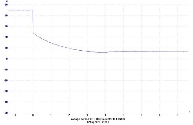
The picture above shows the voltage across TR1 and TR4 at steady state of 46.4V (pos and neg supplies at reduced voltage due to 15 0 15V transformer) just before switch off. At the moment of switch off TR1/TR4 conduct and the voltage drops to about 25V with 22V across the discharge resistors. This quickly drops to around 4-5 Volts.
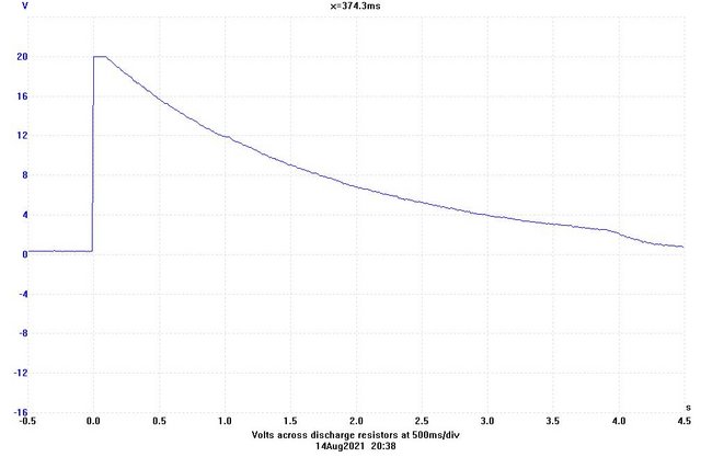
The picture above shows the voltage across the discharge resistors which is zero until the discharge circuit operates when it rises to 22V (unfortunately clipped due to the incorrect scope setting) then smoothly reduced down towards zero.

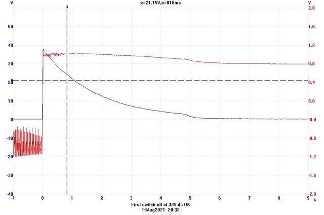
In the picture above the red trace shows the hold off signal at about -1V. When the supply is switched off this quickly rises to 1V positive and initiates the discharge. The blue trace is the voltage across the discharge resistors which jumps from zero to 22V (clipped again due to dodgy scope setting) at the moment of switch off and then reduces slowly as TR1/TR4 control the discharge to near zero at about 9 seconds in.
During these runs I monitored the temperature rise of the 620R discharge resistors but they only rose to about 30C for a few seconds after each switch off then retuned to about 23C. I repeated the switch on/wait/switch off cycle a further 25 times but could not detect any abnormal operation.
Whilst looking for something else I found another transformer 25 0 25V so I thought I would try that although the Naim circuit uses a 22 0 22V on this circuit. When I powered up the TX it actually produced 27 0 27 V which resulted in + - 38VDC. I wired it in and did the first cycle of switch on switch off.
In the picture above the red trace shows the same voltage shift from -1V hold off to plus 1V discharge start. The control signal voltage is very similar even though the circuit is now sat across + - 38V = 76V instead of the previous + - 23.2 + 46.4V. The blue trace shows the voltage across the resistors at the start of discharge is 38V leaving the balance of the voltage 38V across the collectors – emitters of TR1/TR4. The trace looks very similar to the previous ones and all appears OK. The temperature rise across the discharge resistors increased slightly to 34C at each discharge falling quickly as before.
When I switched on for the next cycle I heard a sharp crack and noticed the three discharge resistors near TR4 starting to smoke. I switched off immediately and tried to work out if there was anything different other than running at a higher voltage. When I checked all the components in the trial circuit I found that TR4 had gone short circuit collector to emitter. My first thoughts were that I had over volted the transistors with a higher than normal voltage but when I checked the ZTX 753 is rated at 100V collector-emitter and I am applying 76V at switch on with no current flowing into the discharge resistors (other than an occasional small start up blip I later observed).
I replaced TR4 and checked the other transistors on a Peak component tester which showed they were OK so I put them back in. The three resistors fed from TR4 had changed from 620R to 645R. I didn’t bother to change them yet as I expected further fireworks to follow.
I switched on for the next cycle with some trepidation but it started up OK so after the 30 second wait I switched off again. No fireworks even though it was the same + - 38V supply as the time when it failed. I tried a few more switch on / off cycles and all appeared OK so I decided to continue with another 50 cycles and collect a few scope traces.
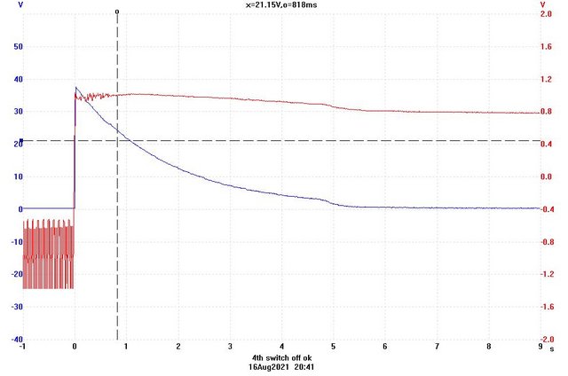
The above picture shows the 4th switch off with the 38V supplies which looks OK but I notice a bit of noise on the red signal trace just after switch off. I rehashed the earths to clean it up a bit.

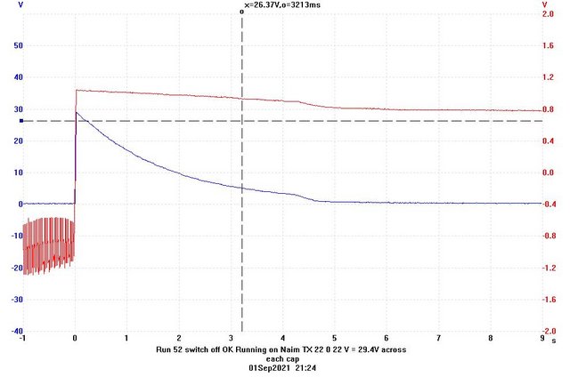
The above picture shows the 31st switch off with the 38V supplies at 5X magnification on the X axis. It covers 1 second either side of the switch off point. The red trace flipping from -1V to +1V at the switch off point and the blue trace showing voltage across the discharge resistors jumping from 0 to 38V then declining. Ignore the dotted cursor line.
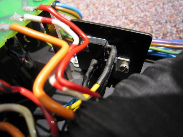
After completing 50 switching cycles on the 15 0 15V transformer and 50 cycles using the 25 0 25V transformer I connected the trial circuit to the 22 0 22V windings of the actual 555PS transformer taking great care to isolate all the other outputs. I still used the trial rectifiers and capacitors so the only thing powered up in the 555PS was the mains transformer and switch. I kept the 555PS main switch closed for all tests and just used the 13A socket switch to minimise wear on the Naim switch.
I powered up the supply and as expected measured 22 0 22V AC at the TX secondary with a smidge under 30V on both Pos and Neg supplies giving 60V across the pair of caps and trial discharge board. I ran the same switch on off routine as before and everything appears to be working OK with no fireworks. The discharge resistors and their switching transistors never exceeded about 35C just after switch off.
The above picture shows the discharge circuit running from the Naim 22 0 22 transformer winding and shows the circuit behaving exactly as the Spice simulations.
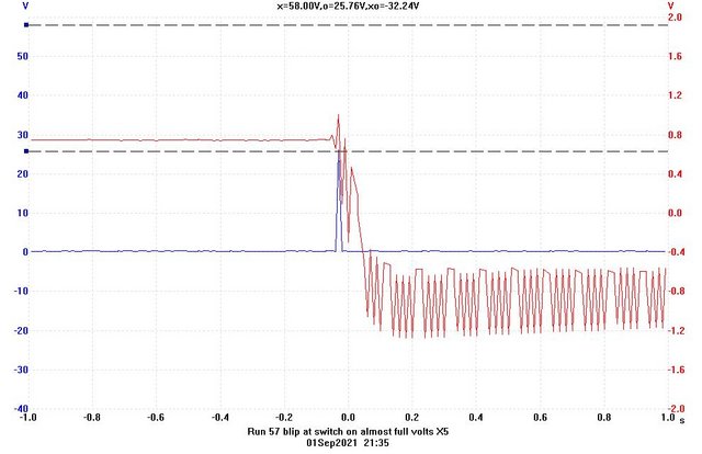
The above picture is quite interesting and confirms that occasionally, possibly depending where in the mains cycle the circuit is switched on, a small blip of current is passed through the discharge resistors during start up. The reason this occurs is residual voltage in the main caps leaves about 0.8V on the hold off circuit trigger signal. When the supply is switched on the negative pulses from D1 drive the signal towards -1V to -1.5V but as can be seen in this start up the red trace has momentarily jumped up to about 1V switching the discharge transistors on for about one cycle. The blue trace shows the voltage across the discharge resistors momentarily rose to about 25V, this one is quite large as most of these blips are about 10V. I first notice this in the Spice simulations which shows what a powerful tool it is. See the spice simulations in posts No. 28 above.
I ran the circuit using the Naim transformer for a total of 200 on/off cycles without incident. I still need to determine the exact cause of the TR4 failure because I believe that is at the heart of why my 555PS failed.
However, just before I started on that I disconnected the links on the trial board feeding the two sets of three small 620R discharge resistors and connected wiring to a pair of T0220 style Bourns 220R 20W resistors. I intend to use these mounted in thermal contact with a manual reset 45C cutout switch. This will provide an early automatic shutdown if a discharge transistor fails short circuit. With the 220R resistors in circuit in place of the 2 x 3 x 620R I ran a further 50 switch on/off cycles without incident. The different resistor values 220R versus 3 x 620R = 207R made no real discernible difference to the discharge circuit operation.
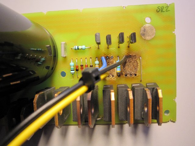
The picture above shows the trial circuit board with the Pos, Neg, OV and transformer 22V wires coming in at the left side. Near the left and right transistors, TR1 and TR4, the links have been removed and wires added ( yellow, black & red) to feed the two off board resistors. The three resistors at the right side can be seen scorched due to the previous failure of TR4 (rightmost – now replaced).
This picture shows the experimental upstand housing the thermal cut out with two high power T0220 resistors mounted on the reverse using the same fixings. The aim here is to provide a quick shutdown should the resistors overheat due to a circuit fault.
To Be Continued……..
After experimenting with the discharge resistors I looked at all the other components in the discharge circuit and despite the severe damage found the only other failed components were the two discharge switching transistors TR1 and TR4 in my sketch (Q3 and Q4 in the Naim drawing). Both of these had burnt out and gone open circuit with TR4 blown in half.
To recap the control signal is derived from the 22V transformer winding via diode D1and resistor R1 and smoothed by C1. It is trimmed via the 4 IN4148 diodes and when the transformer is live produces a -1V hold off signal to the Darlington pair TR2/TR3 which biases the discharge transistors TR1/TR4 off until the transformer output ceases. When the 22v AC goes off the signal rises to just above 1V positive and initiates the discharge.
With all of this is still working OK it looks most unlikely that a failure in this part of the circuit could have caused it to go into discharge mode whilst still on. However, the Spice simulations did show the circuit can go into momentary discharge during the first few cycles at switch on. (This was actually observed in the trial circuit later)
I made up a duplicate circuit for testing on Veroboard using all new parts. The transistors I used are genuine Diodes Inc. ZTX653 NPN for the Darlington pair and ZTX 753 PNP for the discharge switching transistors same as the Naim circuit. I also used a spare pair of Felsic C039 15,00uF caps and the same rectifiers as the 555PS uses.
I initially ran the circuit from a 15V 0 15V transformer mainly because that’s all I had but it actually produces 16.4V 0 16.4V due to regulation. I powered up the circuit and as expected it produced plus and minus 23.2V at the capacitors. Although this was a lower than the plus and minus 30V the circuit normally runs at I was able to monitor the charge and discharge of the two big caps. A few seconds after switch off the caps discharge to 3-4 volts each.
I cycled the circuit on and off 25 times allowing around 30 seconds between each switching operation. I observed the circuit function on a Picoscope ADC 200 and captured a few traces. These proved to be remarkably similar to the Spice simulation pictures I posted earlier especially the slight hump in the discharge curve at 4-5 seconds in.
The picture above shows the voltage across TR1 and TR4 at steady state of 46.4V (pos and neg supplies at reduced voltage due to 15 0 15V transformer) just before switch off. At the moment of switch off TR1/TR4 conduct and the voltage drops to about 25V with 22V across the discharge resistors. This quickly drops to around 4-5 Volts.
The picture above shows the voltage across the discharge resistors which is zero until the discharge circuit operates when it rises to 22V (unfortunately clipped due to the incorrect scope setting) then smoothly reduced down towards zero.
In the picture above the red trace shows the hold off signal at about -1V. When the supply is switched off this quickly rises to 1V positive and initiates the discharge. The blue trace is the voltage across the discharge resistors which jumps from zero to 22V (clipped again due to dodgy scope setting) at the moment of switch off and then reduces slowly as TR1/TR4 control the discharge to near zero at about 9 seconds in.
During these runs I monitored the temperature rise of the 620R discharge resistors but they only rose to about 30C for a few seconds after each switch off then retuned to about 23C. I repeated the switch on/wait/switch off cycle a further 25 times but could not detect any abnormal operation.
Whilst looking for something else I found another transformer 25 0 25V so I thought I would try that although the Naim circuit uses a 22 0 22V on this circuit. When I powered up the TX it actually produced 27 0 27 V which resulted in + - 38VDC. I wired it in and did the first cycle of switch on switch off.
In the picture above the red trace shows the same voltage shift from -1V hold off to plus 1V discharge start. The control signal voltage is very similar even though the circuit is now sat across + - 38V = 76V instead of the previous + - 23.2 + 46.4V. The blue trace shows the voltage across the resistors at the start of discharge is 38V leaving the balance of the voltage 38V across the collectors – emitters of TR1/TR4. The trace looks very similar to the previous ones and all appears OK. The temperature rise across the discharge resistors increased slightly to 34C at each discharge falling quickly as before.
When I switched on for the next cycle I heard a sharp crack and noticed the three discharge resistors near TR4 starting to smoke. I switched off immediately and tried to work out if there was anything different other than running at a higher voltage. When I checked all the components in the trial circuit I found that TR4 had gone short circuit collector to emitter. My first thoughts were that I had over volted the transistors with a higher than normal voltage but when I checked the ZTX 753 is rated at 100V collector-emitter and I am applying 76V at switch on with no current flowing into the discharge resistors (other than an occasional small start up blip I later observed).
I replaced TR4 and checked the other transistors on a Peak component tester which showed they were OK so I put them back in. The three resistors fed from TR4 had changed from 620R to 645R. I didn’t bother to change them yet as I expected further fireworks to follow.
I switched on for the next cycle with some trepidation but it started up OK so after the 30 second wait I switched off again. No fireworks even though it was the same + - 38V supply as the time when it failed. I tried a few more switch on / off cycles and all appeared OK so I decided to continue with another 50 cycles and collect a few scope traces.
The above picture shows the 4th switch off with the 38V supplies which looks OK but I notice a bit of noise on the red signal trace just after switch off. I rehashed the earths to clean it up a bit.
The above picture shows the 31st switch off with the 38V supplies at 5X magnification on the X axis. It covers 1 second either side of the switch off point. The red trace flipping from -1V to +1V at the switch off point and the blue trace showing voltage across the discharge resistors jumping from 0 to 38V then declining. Ignore the dotted cursor line.
After completing 50 switching cycles on the 15 0 15V transformer and 50 cycles using the 25 0 25V transformer I connected the trial circuit to the 22 0 22V windings of the actual 555PS transformer taking great care to isolate all the other outputs. I still used the trial rectifiers and capacitors so the only thing powered up in the 555PS was the mains transformer and switch. I kept the 555PS main switch closed for all tests and just used the 13A socket switch to minimise wear on the Naim switch.
I powered up the supply and as expected measured 22 0 22V AC at the TX secondary with a smidge under 30V on both Pos and Neg supplies giving 60V across the pair of caps and trial discharge board. I ran the same switch on off routine as before and everything appears to be working OK with no fireworks. The discharge resistors and their switching transistors never exceeded about 35C just after switch off.
The above picture shows the discharge circuit running from the Naim 22 0 22 transformer winding and shows the circuit behaving exactly as the Spice simulations.
The above picture is quite interesting and confirms that occasionally, possibly depending where in the mains cycle the circuit is switched on, a small blip of current is passed through the discharge resistors during start up. The reason this occurs is residual voltage in the main caps leaves about 0.8V on the hold off circuit trigger signal. When the supply is switched on the negative pulses from D1 drive the signal towards -1V to -1.5V but as can be seen in this start up the red trace has momentarily jumped up to about 1V switching the discharge transistors on for about one cycle. The blue trace shows the voltage across the discharge resistors momentarily rose to about 25V, this one is quite large as most of these blips are about 10V. I first notice this in the Spice simulations which shows what a powerful tool it is. See the spice simulations in posts No. 28 above.
I ran the circuit using the Naim transformer for a total of 200 on/off cycles without incident. I still need to determine the exact cause of the TR4 failure because I believe that is at the heart of why my 555PS failed.
However, just before I started on that I disconnected the links on the trial board feeding the two sets of three small 620R discharge resistors and connected wiring to a pair of T0220 style Bourns 220R 20W resistors. I intend to use these mounted in thermal contact with a manual reset 45C cutout switch. This will provide an early automatic shutdown if a discharge transistor fails short circuit. With the 220R resistors in circuit in place of the 2 x 3 x 620R I ran a further 50 switch on/off cycles without incident. The different resistor values 220R versus 3 x 620R = 207R made no real discernible difference to the discharge circuit operation.
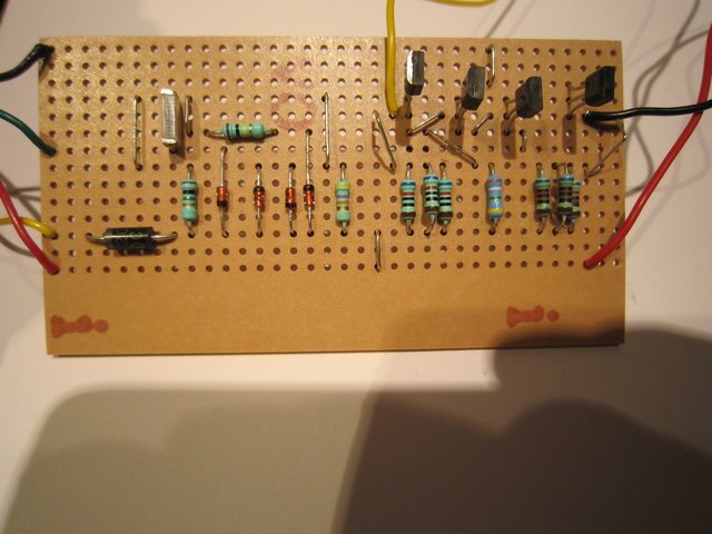
The picture above shows the trial circuit board with the Pos, Neg, OV and transformer 22V wires coming in at the left side. Near the left and right transistors, TR1 and TR4, the links have been removed and wires added ( yellow, black & red) to feed the two off board resistors. The three resistors at the right side can be seen scorched due to the previous failure of TR4 (rightmost – now replaced).
This picture shows the experimental upstand housing the thermal cut out with two high power T0220 resistors mounted on the reverse using the same fixings. The aim here is to provide a quick shutdown should the resistors overheat due to a circuit fault.
To Be Continued……..
neonixcool
pfm Member
Excellent my friend very helpfull information thanks !!!
Thanks my friend !!! Very helpfull informationCaution!.. Long and Rambling Post.
After experimenting with the discharge resistors I looked at all the other components in the discharge circuit and despite the severe damage found the only other failed components were the two discharge switching transistors TR1 and TR4 in my sketch (Q3 and Q4 in the Naim drawing). Both of these had burnt out and gone open circuit with TR4 blown in half.
To recap the control signal is derived from the 22V transformer winding via diode D1and resistor R1 and smoothed by C1. It is trimmed via the 4 IN4148 diodes and when the transformer is live produces a -1V hold off signal to the Darlington pair TR2/TR3 which biases the discharge transistors TR1/TR4 off until the transformer output ceases. When the 22v AC goes off the signal rises to just above 1V positive and initiates the discharge.
With all of this is still working OK it looks most unlikely that a failure in this part of the circuit could have caused it to go into discharge mode whilst still on. However, the Spice simulations did show the circuit can go into momentary discharge during the first few cycles at switch on. (This was actually observed in the trial circuit later)
I made up a duplicate circuit for testing on Veroboard using all new parts. The transistors I used are genuine Diodes Inc. ZTX653 NPN for the Darlington pair and ZTX 753 PNP for the discharge switching transistors same as the Naim circuit. I also used a spare pair of Felsic C039 15,00uF caps and the same rectifiers as the 555PS uses.
I initially ran the circuit from a 15V 0 15V transformer mainly because that’s all I had but it actually produces 16.4V 0 16.4V due to regulation. I powered up the circuit and as expected it produced plus and minus 23.2V at the capacitors. Although this was a lower than the plus and minus 30V the circuit normally runs at I was able to monitor the charge and discharge of the two big caps. A few seconds after switch off the caps discharge to 3-4 volts each.
I cycled the circuit on and off 25 times allowing around 30 seconds between each switching operation. I observed the circuit function on a Picoscope ADC 200 and captured a few traces. These proved to be remarkably similar to the Spice simulation pictures I posted earlier especially the slight hump in the discharge curve at 4-5 seconds in.
The picture above shows the voltage across TR1 and TR4 at steady state of 46.4V (pos and neg supplies at reduced voltage due to 15 0 15V transformer) just before switch off. At the moment of switch off TR1/TR4 conduct and the voltage drops to about 25V with 22V across the discharge resistors. This quickly drops to around 4-5 Volts.
The picture above shows the voltage across the discharge resistors which is zero until the discharge circuit operates when it rises to 22V (unfortunately clipped due to the incorrect scope setting) then smoothly reduced down towards zero.
In the picture above the red trace shows the hold off signal at about -1V. When the supply is switched off this quickly rises to 1V positive and initiates the discharge. The blue trace is the voltage across the discharge resistors which jumps from zero to 22V (clipped again due to dodgy scope setting) at the moment of switch off and then reduces slowly as TR1/TR4 control the discharge to near zero at about 9 seconds in.
During these runs I monitored the temperature rise of the 620R discharge resistors but they only rose to about 30C for a few seconds after each switch off then retuned to about 23C. I repeated the switch on/wait/switch off cycle a further 25 times but could not detect any abnormal operation.
Whilst looking for something else I found another transformer 25 0 25V so I thought I would try that although the Naim circuit uses a 22 0 22V on this circuit. When I powered up the TX it actually produced 27 0 27 V which resulted in + - 38VDC. I wired it in and did the first cycle of switch on switch off.
In the picture above the red trace shows the same voltage shift from -1V hold off to plus 1V discharge start. The control signal voltage is very similar even though the circuit is now sat across + - 38V = 76V instead of the previous + - 23.2 + 46.4V. The blue trace shows the voltage across the resistors at the start of discharge is 38V leaving the balance of the voltage 38V across the collectors – emitters of TR1/TR4. The trace looks very similar to the previous ones and all appears OK. The temperature rise across the discharge resistors increased slightly to 34C at each discharge falling quickly as before.
When I switched on for the next cycle I heard a sharp crack and noticed the three discharge resistors near TR4 starting to smoke. I switched off immediately and tried to work out if there was anything different other than running at a higher voltage. When I checked all the components in the trial circuit I found that TR4 had gone short circuit collector to emitter. My first thoughts were that I had over volted the transistors with a higher than normal voltage but when I checked the ZTX 753 is rated at 100V collector-emitter and I am applying 76V at switch on with no current flowing into the discharge resistors (other than an occasional small start up blip I later observed).
I replaced TR4 and checked the other transistors on a Peak component tester which showed they were OK so I put them back in. The three resistors fed from TR4 had changed from 620R to 645R. I didn’t bother to change them yet as I expected further fireworks to follow.
I switched on for the next cycle with some trepidation but it started up OK so after the 30 second wait I switched off again. No fireworks even though it was the same + - 38V supply as the time when it failed. I tried a few more switch on / off cycles and all appeared OK so I decided to continue with another 50 cycles and collect a few scope traces.
The above picture shows the 4th switch off with the 38V supplies which looks OK but I notice a bit of noise on the red signal trace just after switch off. I rehashed the earths to clean it up a bit.
The above picture shows the 31st switch off with the 38V supplies at 5X magnification on the X axis. It covers 1 second either side of the switch off point. The red trace flipping from -1V to +1V at the switch off point and the blue trace showing voltage across the discharge resistors jumping from 0 to 38V then declining. Ignore the dotted cursor line.
After completing 50 switching cycles on the 15 0 15V transformer and 50 cycles using the 25 0 25V transformer I connected the trial circuit to the 22 0 22V windings of the actual 555PS transformer taking great care to isolate all the other outputs. I still used the trial rectifiers and capacitors so the only thing powered up in the 555PS was the mains transformer and switch. I kept the 555PS main switch closed for all tests and just used the 13A socket switch to minimise wear on the Naim switch.
I powered up the supply and as expected measured 22 0 22V AC at the TX secondary with a smidge under 30V on both Pos and Neg supplies giving 60V across the pair of caps and trial discharge board. I ran the same switch on off routine as before and everything appears to be working OK with no fireworks. The discharge resistors and their switching transistors never exceeded about 35C just after switch off.
The above picture shows the discharge circuit running from the Naim 22 0 22 transformer winding and shows the circuit behaving exactly as the Spice simulations.
The above picture is quite interesting and confirms that occasionally, possibly depending where in the mains cycle the circuit is switched on, a small blip of current is passed through the discharge resistors during start up. The reason this occurs is residual voltage in the main caps leaves about 0.8V on the hold off circuit trigger signal. When the supply is switched on the negative pulses from D1 drive the signal towards -1V to -1.5V but as can be seen in this start up the red trace has momentarily jumped up to about 1V switching the discharge transistors on for about one cycle. The blue trace shows the voltage across the discharge resistors momentarily rose to about 25V, this one is quite large as most of these blips are about 10V. I first notice this in the Spice simulations which shows what a powerful tool it is. See the spice simulations in posts No. 28 above.
I ran the circuit using the Naim transformer for a total of 200 on/off cycles without incident. I still need to determine the exact cause of the TR4 failure because I believe that is at the heart of why my 555PS failed.
However, just before I started on that I disconnected the links on the trial board feeding the two sets of three small 620R discharge resistors and connected wiring to a pair of T0220 style Bourns 220R 20W resistors. I intend to use these mounted in thermal contact with a manual reset 45C cutout switch. This will provide an early automatic shutdown if a discharge transistor fails short circuit. With the 220R resistors in circuit in place of the 2 x 3 x 620R I ran a further 50 switch on/off cycles without incident. The different resistor values 220R versus 3 x 620R = 207R made no real discernible difference to the discharge circuit operation.
The picture above shows the trial circuit board with the Pos, Neg, OV and transformer 22V wires coming in at the left side. Near the left and right transistors, TR1 and TR4, the links have been removed and wires added ( yellow, black & red) to feed the two off board resistors. The three resistors at the right side can be seen scorched due to the previous failure of TR4 (rightmost – now replaced).
This picture shows the experimental upstand housing the thermal cut out with two high power T0220 resistors mounted on the reverse using the same fixings. The aim here is to provide a quick shutdown should the resistors overheat due to a circuit fault.
To Be Continued……..
Cloth Ears
pfm Member
Thanks for the comments - I will post the concluding part soon.
Cloth Ears
pfm Member
The concluding part – please try to stay awake.
I continued running switch on/off cycles using the Naim transformer for a total of 200 cycles monitoring the temperature rise on the switching transistors and the 220R TO220 resistors. The transistor temperature stayed the same at around 36C after each discharge. The resistors never rose above 25C compared to 34C on the small 0.4W resistors but some of this will be down to the slightly higher resistance of the large power resistors 220R compared with 3x680R = 207R. Unfortunately, I could not source the power resistors at 210R but it appears to make little difference and 220R will give the discharge transistors a slightly easier ride.
I next turned my attention to the operation of the thermal trip mounted on the reverse of the power resistors pictured in the previous post. This is Farnell part No. 349-2933 a normally closed 45C manual reset trip rated at 240V 10A AC which I intend to use to shut down the PSU if a control signal/transistor failure causes overheating of the discharge resistors. I noticed some time ago that Naim are using a similar method on certain PSUs but I suspect they are using the NAP 250 style self-resetting trips which will just cycle on/off in the event of a fault.
There are two fault conditions I am trying to protect against:-
Fault condition 1:- Whist the PSU is powered up and any part of the hold off circuit fails the two discharge transistors apply 28V to each discharge resistor simultaneously. Result- the 220R resistors each pass 127mA = 3.55W total 7.1W
Fault condition 2:- Whilst the PSU is powered up and one or both of the discharge switching transistors fails to short circuit applying 60V across one or both resistors. Result – the 220R resistors each pass 272mA = 16.2W for one failed transistor or 32.4W for both transistors failed.
Note the power values are slightly lower than before when using the original 3 x 620R = 207R due to the slightly higher 220R resistance.
The Bourns power resistors are each rated at 2.8W in free air and up to 20W with a suitable heatsink. I have purposely arranged these on a quite small heatsink thermally isolated from the PSU chassis to allow the heat generated to quickly operate the thermal trip and effect the shut down ASAP.
To prove the effectiveness of this circuit I used a bench PSU to apply the 28V or 60V fault voltage to the resistors and a continuity buzzer to detect when the trip had occurred.
For Fault Condition 1 the 28V DC was applied to both 220R resistors simultaneously from room temperature and the time taken for the 45C thermal trip to operate was measured at 47 seconds.
For fault condition 2a the 60V DC was applied to just the upper 220R resistor from room temperature and the time to trip was measured at 24 Seconds.
For fault condition 2b the 60V DC was applied to just the lower 220R resistor from room temperature and the time to trip was measured at 22 Seconds.
For fault condition 2c the 60V DC was applied to both 220R resistors simultaneously from room temperature and the time to trip was measured at 11.9 Seconds.
All the above times were without any heatsink compound just for the trial. I would expect slightly shorter times with compound.
These tests show that if any fault occurs in the -1V hold off circuit then the PSU could shut down in about 47 seconds.
If a single switching transistor were to fail short circuit then a shutdown would occur in about 22 to 24 seconds.
If both switching transistors failed together then a shutdown would occur in about 12 seconds.
I considered this gave robust protection against any future faults so I started to rebuild the original circuit board with all new components.
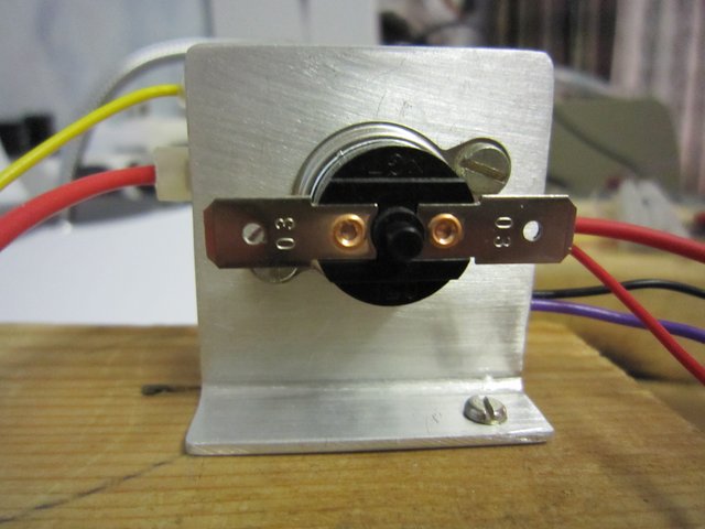
Above is the original PCB after cleaning up and fitted with new components. The three wires connect to the off board high power resistors behind the thermal trip.
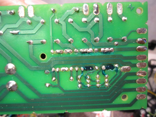
I repaired the printed side of the PCB as best I could but I will probably make a replacement PCB at some point in the future.
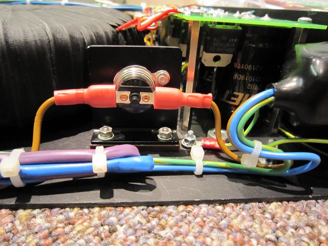
Above is the small heatsink with the discharge power resistors connected on the back. Two layers of heat shrink insulate the connections to the resistors. The metal tabs on the resistors do not require washers as they are electrically isolated with a 4KV dielectric withstand rating.
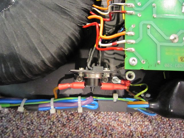
This is an overhead shot showing the heatsink location relative to the PCB with the mains wiring passing handily by. The wiring between the PCB and the power resistors has been kept as short as possible.
This is the front of the heatsink with the 45C trip connected into the live feed from the IEC socket and mains switch. Note the Paxolin thermal insulator at the base of the heatsink to prevent heat being dissipated into the chassis helping to speed up the trip time. There is also a small C shaped Makrolon shroud ( not fitted in this pic) to give finger protection against the two bare terminals. The tiny black reset button from the trip protrudes through a small hole in the shroud.
I fitted the repaired PCB and heatsink assembly with the power resistors but initially left the mains wiring as original. This enabled me to give the modified circuit a good dose of listening to prior to introducing the thermal trip into the mains wire.
I did extensive listening tests for about a week and I quickly came to the conclusion that mounting the discharge resistors a short distance from the PCB had made no difference to the sound whatsoever and it sounds as good as it always has.
I then introduced the cutout switch into the live wire and did further listening tests with either the cutout switch in circuit or a short link with male spades in place of the cutout switch. Once again I could not detect any difference in sound quality and it still sounds superb.
With the NDS /555PS running again I cased it up and put it back in the Fraim rack.
I next turned my attention to what I believe started this saga - the two discharge resistor switching transistors. The transistors are Diodes Incorporated ZTX753, a PNP medium power device rated at 100 Vceo, 2A current and 1W total power. I noticed that the Naim XPS schematic posted by @jpk in post 22 above uses the earlier version of this transistor, the ZTX752, as does my olive Supercap. The main difference between them is the Vceo is only 80V in the ZTX752 compared to 100V in the ZTX753. The data sheet shows the ZTX752 is not recommended for new designs.
At first glance this tiny E line transistor appears well rated for the job but the more I studied the data sheet the less convinced I am that it’s really man enough for the job.
The Vceo rating of 100V appears OK versus the 60V that normally sits across collector and emitter but looking at the safe operating area (SOA) graph in the data sheet reveals that at 60V the collector current must not exceed 20mA continuously or 70mA for 1 second. The instant the discharge is initiated the current drawn by the trio of resistors jumps to 135 mA but at the same time the voltage across the transistor rapidly drops from 60V to 32V. According to the SOA this condition is only valid for 0.1 second. I found it impossible to verify precisely what happens in that transient state when the transistor switches and the current is rising and the voltage is falling.
I also noticed from the data sheet that the relationship between Vceo and collector current is quite limiting i.e.:-
Vce =100V but only at 10mA.
Continuous current rating = 2A but only at 0.5V Vce
Pulse current rating = 6A but only for a very brief 100 uS
Most of the limitation appears to be due to the maximum power rating of 1W but when the discharge first operates 32V x 135mA = 4.32W. This does diminish quite quickly but heats the transistor from 23C to 36C after each discharge in just a few seconds.
During my initial experimentation with a trial discharge circuit I had an early failure of one of the discharge transistors when using a transformer with a higher output voltage than the Naim unit. 27V 0 27V versus 22V 0 22V for the Naim TX.
The 27V 0 27V TX produced 76V DC across the caps and transistors compared with 60V DC from the 22V 0 22V Naim TX and raised the voltage across the transistor during discharge to 38V compared with 32V from the Naim TX.
I reconfigured the trial circuit again with the 100VA 27V 0 27V transformer and a new pair of transistors and repeated the on/wait/off cycles again. I only got to 35 cycles when I short circuited another transistor with a sharp click and started cooking the small resistors again.
One of my main concerns for these tiny transistors is they are sat on the rectifier outputs from the secondary of quite a large transformer and goodness know how much transient EMF they are subjected to during switch on and switch off. I know they are protected by a pair of very beefy 15,000uF caps but I think at some point they are being overvolted causing the transistors to fail.
One particular situation springs to mind which others may have experienced is where you go to switch on the PSU but you don’t push the button in quite far enough and it fails to latch and pops back out. The natural response is to push it straight in again but that is possibly the worst thing to do. I would suggest being careful when switching on this or any other piece of Naim equipment and ensure the switch latches correctly. If not just leave it a few seconds before pressing it again.
During the first couple of seconds after switch on the transformer magnetizing current is building up which is particularly high in a toroidal transformer. This field will momentarily collapse as the switch opens again only to be re-energised a moment later creating voltage spikes on the secondary.
To simulate this I introduced a 2 pole control panel type momentary push button switch into the primary transformer feed. I pressed the button then released it almost straight away then pressed the button again within less than a second. I held the button in for around 30 seconds before releasing it and initiating the discharge. I waited for the transistors to cool between each cycle before repeating. I found that I could reliably damage a transistor within about 20 cycles with this rather brutal test.
Of course these tests with the 27V 0 27V TX are subjecting the transistors to voltages outside the Naim design but I believe their choice of transistor leaves little headroom for any over voltage situations such as switching transients or mains borne voltage spikes which I believe are the root cause of the problem.
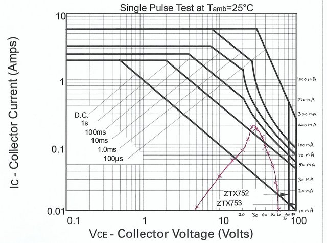
The picture above shows the safe operating area graph taken from the ZTX753 data sheet. The red line at the bottom, which starts at 60V peaks then decays to the left, attempts to show points of voltage and current during the normal switch off discharge curve from the standard Naim circuit using the 22V 0 22V Naim TX. The red line can be seen to cross the DC or continuous line and just cross into the 1 second line. It gets close to but does not cross the O.1 second line. This all looks a bit too close for me but I will confess I’m no expert in SOA graphs.
I did have a brief look for a higher rated transistor but it seems to lurch straight into high voltage high current devices from this point forwards so I have decided to stick with the ZTX753s for now and see how it performs safe in the knowledge that I have a fairly robust safety circuit with the thermal trip cutout.
There are obviously many 555PS DR units out there working perfectly fine. They may also be a few still powering Naim components perfectly OK but have suffered the same fate as mine and have a rather nasty burn out hidden under the PCB. It may be worth checking for signs of overheating on the PCB around the busy section but only by looking at the component side of the rectifier board will you know for sure.
Thanks for reading - now I’ll get back to looking at making that 555PS clone which is where this all started.
I continued running switch on/off cycles using the Naim transformer for a total of 200 cycles monitoring the temperature rise on the switching transistors and the 220R TO220 resistors. The transistor temperature stayed the same at around 36C after each discharge. The resistors never rose above 25C compared to 34C on the small 0.4W resistors but some of this will be down to the slightly higher resistance of the large power resistors 220R compared with 3x680R = 207R. Unfortunately, I could not source the power resistors at 210R but it appears to make little difference and 220R will give the discharge transistors a slightly easier ride.
I next turned my attention to the operation of the thermal trip mounted on the reverse of the power resistors pictured in the previous post. This is Farnell part No. 349-2933 a normally closed 45C manual reset trip rated at 240V 10A AC which I intend to use to shut down the PSU if a control signal/transistor failure causes overheating of the discharge resistors. I noticed some time ago that Naim are using a similar method on certain PSUs but I suspect they are using the NAP 250 style self-resetting trips which will just cycle on/off in the event of a fault.
There are two fault conditions I am trying to protect against:-
Fault condition 1:- Whist the PSU is powered up and any part of the hold off circuit fails the two discharge transistors apply 28V to each discharge resistor simultaneously. Result- the 220R resistors each pass 127mA = 3.55W total 7.1W
Fault condition 2:- Whilst the PSU is powered up and one or both of the discharge switching transistors fails to short circuit applying 60V across one or both resistors. Result – the 220R resistors each pass 272mA = 16.2W for one failed transistor or 32.4W for both transistors failed.
Note the power values are slightly lower than before when using the original 3 x 620R = 207R due to the slightly higher 220R resistance.
The Bourns power resistors are each rated at 2.8W in free air and up to 20W with a suitable heatsink. I have purposely arranged these on a quite small heatsink thermally isolated from the PSU chassis to allow the heat generated to quickly operate the thermal trip and effect the shut down ASAP.
To prove the effectiveness of this circuit I used a bench PSU to apply the 28V or 60V fault voltage to the resistors and a continuity buzzer to detect when the trip had occurred.
For Fault Condition 1 the 28V DC was applied to both 220R resistors simultaneously from room temperature and the time taken for the 45C thermal trip to operate was measured at 47 seconds.
For fault condition 2a the 60V DC was applied to just the upper 220R resistor from room temperature and the time to trip was measured at 24 Seconds.
For fault condition 2b the 60V DC was applied to just the lower 220R resistor from room temperature and the time to trip was measured at 22 Seconds.
For fault condition 2c the 60V DC was applied to both 220R resistors simultaneously from room temperature and the time to trip was measured at 11.9 Seconds.
All the above times were without any heatsink compound just for the trial. I would expect slightly shorter times with compound.
These tests show that if any fault occurs in the -1V hold off circuit then the PSU could shut down in about 47 seconds.
If a single switching transistor were to fail short circuit then a shutdown would occur in about 22 to 24 seconds.
If both switching transistors failed together then a shutdown would occur in about 12 seconds.
I considered this gave robust protection against any future faults so I started to rebuild the original circuit board with all new components.
Above is the original PCB after cleaning up and fitted with new components. The three wires connect to the off board high power resistors behind the thermal trip.
I repaired the printed side of the PCB as best I could but I will probably make a replacement PCB at some point in the future.
Above is the small heatsink with the discharge power resistors connected on the back. Two layers of heat shrink insulate the connections to the resistors. The metal tabs on the resistors do not require washers as they are electrically isolated with a 4KV dielectric withstand rating.
This is an overhead shot showing the heatsink location relative to the PCB with the mains wiring passing handily by. The wiring between the PCB and the power resistors has been kept as short as possible.
This is the front of the heatsink with the 45C trip connected into the live feed from the IEC socket and mains switch. Note the Paxolin thermal insulator at the base of the heatsink to prevent heat being dissipated into the chassis helping to speed up the trip time. There is also a small C shaped Makrolon shroud ( not fitted in this pic) to give finger protection against the two bare terminals. The tiny black reset button from the trip protrudes through a small hole in the shroud.
I fitted the repaired PCB and heatsink assembly with the power resistors but initially left the mains wiring as original. This enabled me to give the modified circuit a good dose of listening to prior to introducing the thermal trip into the mains wire.
I did extensive listening tests for about a week and I quickly came to the conclusion that mounting the discharge resistors a short distance from the PCB had made no difference to the sound whatsoever and it sounds as good as it always has.
I then introduced the cutout switch into the live wire and did further listening tests with either the cutout switch in circuit or a short link with male spades in place of the cutout switch. Once again I could not detect any difference in sound quality and it still sounds superb.
With the NDS /555PS running again I cased it up and put it back in the Fraim rack.
I next turned my attention to what I believe started this saga - the two discharge resistor switching transistors. The transistors are Diodes Incorporated ZTX753, a PNP medium power device rated at 100 Vceo, 2A current and 1W total power. I noticed that the Naim XPS schematic posted by @jpk in post 22 above uses the earlier version of this transistor, the ZTX752, as does my olive Supercap. The main difference between them is the Vceo is only 80V in the ZTX752 compared to 100V in the ZTX753. The data sheet shows the ZTX752 is not recommended for new designs.
At first glance this tiny E line transistor appears well rated for the job but the more I studied the data sheet the less convinced I am that it’s really man enough for the job.
The Vceo rating of 100V appears OK versus the 60V that normally sits across collector and emitter but looking at the safe operating area (SOA) graph in the data sheet reveals that at 60V the collector current must not exceed 20mA continuously or 70mA for 1 second. The instant the discharge is initiated the current drawn by the trio of resistors jumps to 135 mA but at the same time the voltage across the transistor rapidly drops from 60V to 32V. According to the SOA this condition is only valid for 0.1 second. I found it impossible to verify precisely what happens in that transient state when the transistor switches and the current is rising and the voltage is falling.
I also noticed from the data sheet that the relationship between Vceo and collector current is quite limiting i.e.:-
Vce =100V but only at 10mA.
Continuous current rating = 2A but only at 0.5V Vce
Pulse current rating = 6A but only for a very brief 100 uS
Most of the limitation appears to be due to the maximum power rating of 1W but when the discharge first operates 32V x 135mA = 4.32W. This does diminish quite quickly but heats the transistor from 23C to 36C after each discharge in just a few seconds.
During my initial experimentation with a trial discharge circuit I had an early failure of one of the discharge transistors when using a transformer with a higher output voltage than the Naim unit. 27V 0 27V versus 22V 0 22V for the Naim TX.
The 27V 0 27V TX produced 76V DC across the caps and transistors compared with 60V DC from the 22V 0 22V Naim TX and raised the voltage across the transistor during discharge to 38V compared with 32V from the Naim TX.
I reconfigured the trial circuit again with the 100VA 27V 0 27V transformer and a new pair of transistors and repeated the on/wait/off cycles again. I only got to 35 cycles when I short circuited another transistor with a sharp click and started cooking the small resistors again.
One of my main concerns for these tiny transistors is they are sat on the rectifier outputs from the secondary of quite a large transformer and goodness know how much transient EMF they are subjected to during switch on and switch off. I know they are protected by a pair of very beefy 15,000uF caps but I think at some point they are being overvolted causing the transistors to fail.
One particular situation springs to mind which others may have experienced is where you go to switch on the PSU but you don’t push the button in quite far enough and it fails to latch and pops back out. The natural response is to push it straight in again but that is possibly the worst thing to do. I would suggest being careful when switching on this or any other piece of Naim equipment and ensure the switch latches correctly. If not just leave it a few seconds before pressing it again.
During the first couple of seconds after switch on the transformer magnetizing current is building up which is particularly high in a toroidal transformer. This field will momentarily collapse as the switch opens again only to be re-energised a moment later creating voltage spikes on the secondary.
To simulate this I introduced a 2 pole control panel type momentary push button switch into the primary transformer feed. I pressed the button then released it almost straight away then pressed the button again within less than a second. I held the button in for around 30 seconds before releasing it and initiating the discharge. I waited for the transistors to cool between each cycle before repeating. I found that I could reliably damage a transistor within about 20 cycles with this rather brutal test.
Of course these tests with the 27V 0 27V TX are subjecting the transistors to voltages outside the Naim design but I believe their choice of transistor leaves little headroom for any over voltage situations such as switching transients or mains borne voltage spikes which I believe are the root cause of the problem.
The picture above shows the safe operating area graph taken from the ZTX753 data sheet. The red line at the bottom, which starts at 60V peaks then decays to the left, attempts to show points of voltage and current during the normal switch off discharge curve from the standard Naim circuit using the 22V 0 22V Naim TX. The red line can be seen to cross the DC or continuous line and just cross into the 1 second line. It gets close to but does not cross the O.1 second line. This all looks a bit too close for me but I will confess I’m no expert in SOA graphs.
I did have a brief look for a higher rated transistor but it seems to lurch straight into high voltage high current devices from this point forwards so I have decided to stick with the ZTX753s for now and see how it performs safe in the knowledge that I have a fairly robust safety circuit with the thermal trip cutout.
There are obviously many 555PS DR units out there working perfectly fine. They may also be a few still powering Naim components perfectly OK but have suffered the same fate as mine and have a rather nasty burn out hidden under the PCB. It may be worth checking for signs of overheating on the PCB around the busy section but only by looking at the component side of the rectifier board will you know for sure.
Thanks for reading - now I’ll get back to looking at making that 555PS clone which is where this all started.
Last edited:
rontoolsie
pfm Member
The concluding part – please try to stay awake.
That is excellent information-you are obviously comitted to the 555PS. Even if you eventually build a My-Cap, you have learned what not to do.
neonixcool
pfm Member
Good dayThe concluding part – please try to stay awake.
I continued running switch on/off cycles using the Naim transformer for a total of 200 cycles monitoring the temperature rise on the switching transistors and the 220R TO220 resistors. The transistor temperature stayed the same at around 36C after each discharge. The resistors never rose above 25C compared to 34C on the small 0.4W resistors but some of this will be down to the slightly higher resistance of the large power resistors 220R compared with 3x680R = 207R. Unfortunately, I could not source the power resistors at 210R but it appears to make little difference and 220R will give the discharge transistors a slightly easier ride.
I next turned my attention to the operation of the thermal trip mounted on the reverse of the power resistors pictured in the previous post. This is Farnell part No. 349-2933 a normally closed 45C manual reset trip rated at 240V 10A AC which I intend to use to shut down the PSU if a control signal/transistor failure causes overheating of the discharge resistors. I noticed some time ago that Naim are using a similar method on certain PSUs but I suspect they are using the NAP 250 style self-resetting trips which will just cycle on/off in the event of a fault.
There are two fault conditions I am trying to protect against:-
Fault condition 1:- Whist the PSU is powered up and any part of the hold off circuit fails the two discharge transistors apply 28V to each discharge resistor simultaneously. Result- the 220R resistors each pass 127mA = 3.55W total 7.1W
Fault condition 2:- Whilst the PSU is powered up and one or both of the discharge switching transistors fails to short circuit applying 60V across one or both resistors. Result – the 220R resistors each pass 272mA = 16.2W for one failed transistor or 32.4W for both transistors failed.
Note the power values are slightly lower than before when using the original 3 x 620R = 207R due to the slightly higher 220R resistance.
The Bourns power resistors are each rated at 2.8W in free air and up to 20W with a suitable heatsink. I have purposely arranged these on a quite small heatsink thermally isolated from the PSU chassis to allow the heat generated to quickly operate the thermal trip and effect the shut down ASAP.
To prove the effectiveness of this circuit I used a bench PSU to apply the 28V or 60V fault voltage to the resistors and a continuity buzzer to detect when the trip had occurred.
For Fault Condition 1 the 28V DC was applied to both 220R resistors simultaneously from room temperature and the time taken for the 45C thermal trip to operate was measured at 47 seconds.
For fault condition 2a the 60V DC was applied to just the upper 220R resistor from room temperature and the time to trip was measured at 24 Seconds.
For fault condition 2b the 60V DC was applied to just the lower 220R resistor from room temperature and the time to trip was measured at 22 Seconds.
For fault condition 2c the 60V DC was applied to both 220R resistors simultaneously from room temperature and the time to trip was measured at 11.9 Seconds.
All the above times were without any heatsink compound just for the trial. I would expect slightly shorter times with compound.
These tests show that if any fault occurs in the -1V hold off circuit then the PSU could shut down in about 47 seconds.
If a single switching transistor were to fail short circuit then a shutdown would occur in about 22 to 24 seconds.
If both switching transistors failed together then a shutdown would occur in about 12 seconds.
I considered this gave robust protection against any future faults so I started to rebuild the original circuit board with all new components.
Above is the original PCB after cleaning up and fitted with new components. The three wires connect to the off board high power resistors behind the thermal trip.
I repaired the printed side of the PCB as best I could but I will probably make a replacement PCB at some point in the future.
Above is the small heatsink with the discharge power resistors connected on the back. Two layers of heat shrink insulate the connections to the resistors. The metal tabs on the resistors do not require washers as they are electrically isolated with a 4KV dielectric withstand rating.
This is an overhead shot showing the heatsink location relative to the PCB with the mains wiring passing handily by. The wiring between the PCB and the power resistors has been kept as short as possible.
This is the front of the heatsink with the 45C trip connected into the live feed from the IEC socket and mains switch. Note the Paxolin thermal insulator at the base of the heatsink to prevent heat being dissipated into the chassis helping to speed up the trip time. There is also a small C shaped Makrolon shroud ( not fitted in this pic) to give finger protection against the two bare terminals. The tiny black reset button from the trip protrudes through a small hole in the shroud.
I fitted the repaired PCB and heatsink assembly with the power resistors but initially left the mains wiring as original. This enabled me to give the modified circuit a good dose of listening to prior to introducing the thermal trip into the mains wire.
I did extensive listening tests for about a week and I quickly came to the conclusion that mounting the discharge resistors a short distance from the PCB had made no difference to the sound whatsoever and it sounds as good as it always has.
I then introduced the cutout switch into the live wire and did further listening tests with either the cutout switch in circuit or a short link with male spades in place of the cutout switch. Once again I could not detect any difference in sound quality and it still sounds superb.
With the NDS /555PS running again I cased it up and put it back in the Fraim rack.
I next turned my attention to what I believe started this saga - the two discharge resistor switching transistors. The transistors are Diodes Incorporated ZTX753, a PNP medium power device rated at 100 Vceo, 2A current and 1W total power. I noticed that the Naim XPS schematic posted by @jpk in post 22 above uses the earlier version of this transistor, the ZTX752, as does my olive Supercap. The main difference between them is the Vceo is only 80V in the ZTX752 compared to 100V in the ZTX753. The data sheet shows the ZTX752 is not recommended for new designs.
At first glance this tiny E line transistor appears well rated for the job but the more I studied the data sheet the less convinced I am that it’s really man enough for the job.
The Vceo rating of 100V appears OK versus the 60V that normally sits across collector and emitter but looking at the safe operating area (SOA) graph in the data sheet reveals that at 60V the collector current must not exceed 20mA continuously or 70mA for 1 second. The instant the discharge is initiated the current drawn by the trio of resistors jumps to 135 mA but at the same time the voltage across the transistor rapidly drops from 60V to 32V. According to the SOA this condition is only valid for 0.1 second. I found it impossible to verify precisely what happens in that transient state when the transistor switches and the current is rising and the voltage is falling.
I also noticed from the data sheet that the relationship between Vceo and collector current is quite limiting i.e.:-
Vce =100V but only at 10mA.
Continuous current rating = 2A but only at 0.5V Vce
Pulse current rating = 6A but only for a very brief 100 uS
Most of the limitation appears to be due to the maximum power rating of 1W but when the discharge first operates 32V x 135mA = 4.32W. This does diminish quite quickly but heats the transistor from 23C to 36C after each discharge in just a few seconds.
During my initial experimentation with a trial discharge circuit I had an early failure of one of the discharge transistors when using a transformer with a higher output voltage than the Naim unit. 27V 0 27V versus 22V 0 22V for the Naim TX.
The 27V 0 27V TX produced 76V DC across the caps and transistors compared with 60V DC from the 22V 0 22V Naim TX and raised the voltage across the transistor during discharge to 38V compared with 32V from the Naim TX.
I reconfigured the trial circuit again with the 100VA 27V 0 27V transformer and a new pair of transistors and repeated the on/wait/off cycles again. I only got to 35 cycles when I short circuited another transistor with a sharp click and started cooking the small resistors again.
One of my main concerns for these tiny transistors is they are sat on the rectifier outputs from the secondary of quite a large transformer and goodness know how much transient EMF they are subjected to during switch on and switch off. I know they are protected by a pair of very beefy 15,000uF caps but I think at some point they are being overvolted causing the transistors to fail.
One particular situation springs to mind which others may have experienced is where you go to switch on the PSU but you don’t push the button in quite far enough and it fails to latch and pops back out. The natural response is to push it straight in again but that is possibly the worst thing to do. I would suggest being careful when switching on this or any other piece of Naim equipment and ensure the switch latches correctly. If not just leave it a few seconds before pressing it again.
During the first couple of seconds after switch on the transformer magnetizing current is building up which is particularly high in a toroidal transformer. This field will momentarily collapse as the switch opens again only to be re-energised a moment later creating voltage spikes on the secondary.
To simulate this I introduced a 2 pole control panel type momentary push button switch into the primary transformer feed. I pressed the button then released it almost straight away then pressed the button again within less than a second. I held the button in for around 30 seconds before releasing it and initiating the discharge. I waited for the transistors to cool between each cycle before repeating. I found that I could reliably damage a transistor within about 20 cycles with this rather brutal test.
Of course these tests with the 27V 0 27V TX are subjecting the transistors to voltages outside the Naim design but I believe their choice of transistor leaves little headroom for any over voltage situations such as switching transients or mains borne voltage spikes which I believe are the root cause of the problem.
The picture above shows the safe operating area graph taken from the ZTX753 data sheet. The red line at the bottom, which starts at 60V peaks then decays to the left, attempts to show points of voltage and current during the normal switch off discharge curve from the standard Naim circuit using the 22V 0 22V Naim TX. The red line can be seen to cross the DC or continuous line and just cross into the 1 second line. It gets close to but does not cross the O.1 second line. This all looks a bit too close for me but I will confess I’m no expert in SOA graphs.
I did have a brief look for a higher rated transistor but it seems to lurch straight into high voltage high current devices from this point forwards so I have decided to stick with the ZTX753s for now and see how it performs safe in the knowledge that I have a fairly robust safety circuit with the thermal trip cutout.
There are obviously many 555PS DR units out there working perfectly fine. They may also be a few still powering Naim components perfectly OK but have suffered the same fate as mine and have a rather nasty burn out hidden under the PCB. It may be worth checking for signs of overheating on the PCB around the busy section but only by looking at the component side of the rectifier board will you know for sure.
Thanks for reading - now I’ll get back to looking at making that 555PS clone which is where this all started.
Maybe good idea the added to this solution MCU Atmel Attiny13A for switching the ztx transistors
with simple programm for delay start when PSU is power on
Or just parallel two ztx for increase the power switching
Qwin
pfm Member
Wow, that was some break down, hope you manage to rectify it.Well luckily the whole Twin Towers Naim rack was not quite a blazing inferno but I have discovered a seriously burnt out section of circuit board within the 555PS DR feeding my NDS which is very alarming. This is the circuit responsible for discharging the pair of 15,000 uF capacitors feeding the split voltage analogue supply regulators which has seriously overheated and burnt the PCB, capacitor discharge resistors and controlling transistors.
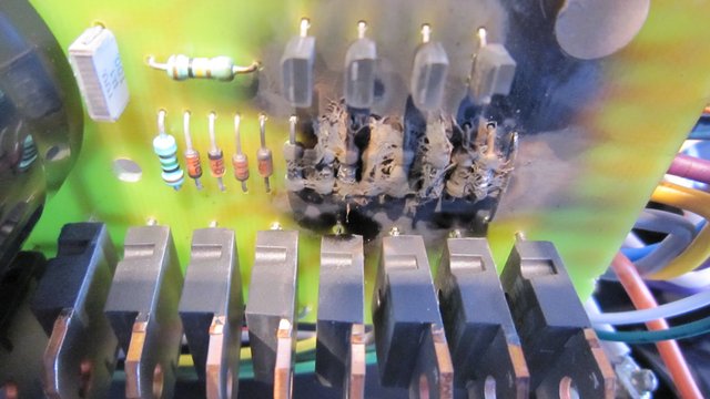
I discovered this damage quite by chance after I was inspired by some old posts from 2018, 2019 and 2020 on the advantages of adding a second PSU on the NDS and ND555 streamers. The second power supply feeds the analogue and separates it from the digital supply. There was discussion around using Teddy Pardo or Naim PSUs and various Burndys.
I opened up the 555PS DR to check out the wiring to the second Burndy socket with a view to making a clone of the 555PS containing just a transformer, rectifier board, 2 capacitors, 2 regulators and a single Burndy socket which looks quite doable.
When I inspected the rectifier board I noticed how brown it was around the busy section nearest to where the DC wiring leaves the board. I removed the PCB to have a look underneath and was horrified to see the resistors and transistors well fried. The amazing part is the 555 PS and NDS work just fine and sounds great. I have measured all the supplies from the transformer right through to the Burndy output pins and everything is running OK.
The Rectifier board is quite simple and comprises of 7 pairs of diodes feeding 2 onboard smoothing capacitors and 5 screw terminal caps off board. I gave it a good dose of reverse engineering and drew out the circuit which has given up the magic smoke. After cleaning it up a bit I can read the part numbers on the 4 transistors and identify most of the other parts but the 7 resistors in the photo below have lost their coding rings. Can anyone with a 555PS help identify their value please. You will need to remove the 5 small torx screws before turning it up from the rear of the chassis. These are the 7 resistors which I need the values for in the picture below.
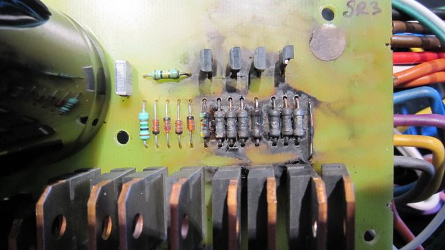
Prior to cleaning up the damaged area I tried to measure the 7 resistors but as expected got very variable results. The 7 damaged ones are a group of 3 low value in parallel, a single high value, then another group of 3 low value in parallel. Discounting the scorched 47K resistor they measured 22R across the left group of 3, then 2 - 3M for the one in the center and 22R across the right group of 3. This would put each resistor in the two groups of 3 at 68R each. The following picture is the discharge circuit as I have drawn it out and this is how I think it works.
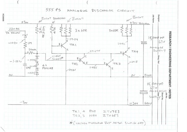
At the left side a 22V AC feed from the same windings supplying the rectifiers and 15,000 uF capacitors for the analogue circuit is rectified and trimmed to -1V by the 4 small diodes. This negative voltage is applied to the base of TR2 which forms a Darlington pair with TR3. The collector of TR3 holds the bases of TR1 and TR4 so they are biased off and the capacitors run at their full voltage of + and – 30V.
When the power supply is turned off the voltage at the four diodes is no longer negative and is pulled up to + 1V by the high value 2 – 3M resistor. This stops TR3 collector from holding the bases of TR1 and TR4 down and they are pulled up by the 47K resistor from the +30V rail. This causes TR1 and TR4 to switch the 2 groups of 68R resistors between the +30V and -30V rails discharging the two 15,000 uF capacitors. Obviously the transistors are now toast so the circuit cannot function correctly but I can still measure the voltage at the base of TR2 flip from -1V to +1V at the moment of switch off.
There is an almost identical three transistor circuit in my olive Supercap with fewer components and just one transistor connecting two 470R resistors in parallel across the single 10,000 uF capacitor which feeds the 12V / 24V regulators for the control supplies. The Supercap discharge circuit is around 22 years old and has been on and off more times than a whores draws without any problems.
In the 555PS I am assuming at least one of the transistors has gone faulty at some point and allowed the bases of TR1 and TR2 to be pulled high switching the resistors across the supply whilst the 555PS is still on causing a major overheat and luckily it did not set the house on fire.
I am particularly keen to know the exact value of the two groups of discharge resistors because this will tell me where Naim have pitched this circuit. From my measurements of the blackened resistors they appear to be three 68R in parallel which means TR1 and TR4 are each switching 60V across 22R7 at the moment of power off. This will cause the tiny transistors to carry 2.67 A each at the moment of initial discharge. The data sheet for these ZTX753 shows absolute max of 2A but also states up to 6A pulse. From the resistor point of view if these are 68R each and I’m driving my Abacus correctly they will be asked to pass 0.8823 A at the moment of switch off and dissipate a momentary 53 Watts each. No wonder they complained.
Can anyone shed any light as to why this circuit exists. I can appreciate that in the case of the S/Cap there would be a desire to drop out the control/mute relays etc. as the voltage rails fall but cannot see how this fits in with the NDS /ND555 analogue circuits unless it’s a legacy from the CD 555 which this supply was originally designed for.
Hope you can help.
Thanks.