Cloth Ears
pfm Member
Well luckily the whole Twin Towers Naim rack was not quite a blazing inferno but I have discovered a seriously burnt out section of circuit board within the 555PS DR feeding my NDS which is very alarming. This is the circuit responsible for discharging the pair of 15,000 uF capacitors feeding the split voltage analogue supply regulators which has seriously overheated and burnt the PCB, capacitor discharge resistors and controlling transistors.
I discovered this damage quite by chance after I was inspired by some old posts from 2018, 2019 and 2020 on the advantages of adding a second PSU on the NDS and ND555 streamers. The second power supply feeds the analogue and separates it from the digital supply. There was discussion around using Teddy Pardo or Naim PSUs and various Burndys.
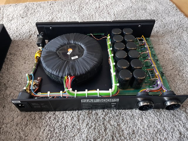
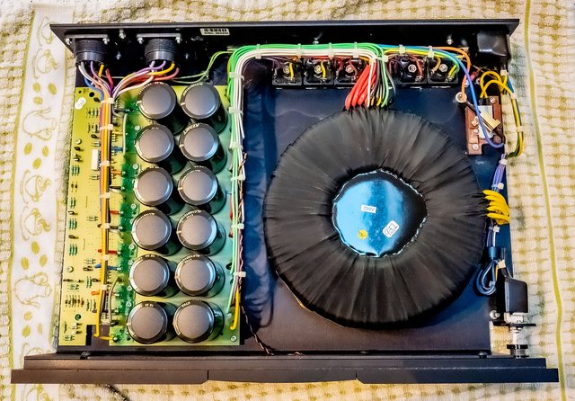
I opened up the 555PS DR to check out the wiring to the second Burndy socket with a view to making a clone of the 555PS containing just a transformer, rectifier board, 2 capacitors, 2 regulators and a single Burndy socket which looks quite doable.
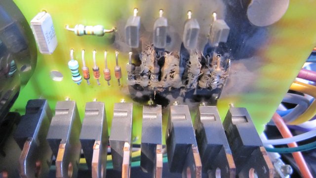
When I inspected the rectifier board I noticed how brown it was around the busy section nearest to where the DC wiring leaves the board. I removed the PCB to have a look underneath and was horrified to see the resistors and transistors well fried. The amazing part is the 555 PS and NDS work just fine and sounds great. I have measured all the supplies from the transformer right through to the Burndy output pins and everything is running OK.
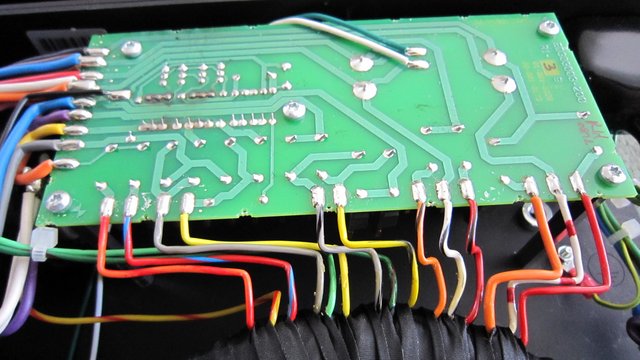
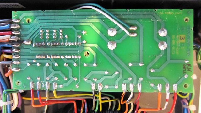
The Rectifier board is quite simple and comprises of 7 pairs of diodes feeding 2 onboard smoothing capacitors and 5 screw terminal caps off board. I gave it a good dose of reverse engineering and drew out the circuit which has given up the magic smoke. After cleaning it up a bit I can read the part numbers on the 4 transistors and identify most of the other parts but the 7 resistors in the photo below have lost their coding rings. Can anyone with a 555PS help identify their value please. You will need to remove the 5 small torx screws before turning it up from the rear of the chassis. These are the 7 resistors which I need the values for in the picture below.
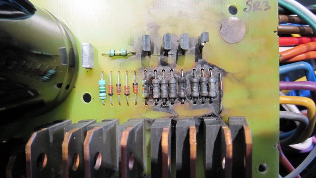
Prior to cleaning up the damaged area I tried to measure the 7 resistors but as expected got very variable results. The 7 damaged ones are a group of 3 low value in parallel, a single high value, then another group of 3 low value in parallel. Discounting the scorched 47K resistor they measured 22R across the left group of 3, then 2 - 3M for the one in the center and 22R across the right group of 3. This would put each resistor in the two groups of 3 at 68R each. The following picture is the discharge circuit as I have drawn it out and this is how I think it works.
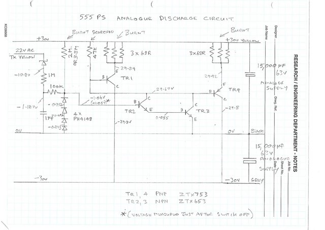
At the left side a 22V AC feed from the same windings supplying the rectifiers and 15,000 uF capacitors for the analogue circuit is rectified and trimmed to -1V by the 4 small diodes. This negative voltage is applied to the base of TR2 which forms a Darlington pair with TR3. The collector of TR3 holds the bases of TR1 and TR4 so they are biased off and the capacitors run at their full voltage of + and – 30V.
When the power supply is turned off the voltage at the four diodes is no longer negative and is pulled up to + 1V by the high value 2 – 3M resistor. This stops TR3 collector from holding the bases of TR1 and TR4 down and they are pulled up by the 47K resistor from the +30V rail. This causes TR1 and TR4 to switch the 2 groups of 68R resistors between the +30V and -30V rails discharging the two 15,000 uF capacitors. Obviously the transistors are now toast so the circuit cannot function correctly but I can still measure the voltage at the base of TR2 flip from -1V to +1V at the moment of switch off.
There is an almost identical three transistor circuit in my olive Supercap with fewer components and just one transistor connecting two 470R resistors in parallel across the single 10,000 uF capacitor which feeds the 12V / 24V regulators for the control supplies. The Supercap discharge circuit is around 22 years old and has been on and off more times than a whores draws without any problems.
In the 555PS I am assuming at least one of the transistors has gone faulty at some point and allowed the bases of TR1 and TR2 to be pulled high switching the resistors across the supply whilst the 555PS is still on causing a major overheat and luckily it did not set the house on fire.
I am particularly keen to know the exact value of the two groups of discharge resistors because this will tell me where Naim have pitched this circuit. From my measurements of the blackened resistors they appear to be three 68R in parallel which means TR1 and TR4 are each switching 60V across 22R7 at the moment of power off. This will cause the tiny transistors to carry 2.67 A each at the moment of initial discharge. The data sheet for these ZTX753 shows absolute max of 2A but also states up to 6A pulse. From the resistor point of view if these are 68R each and I’m driving my Abacus correctly they will be asked to pass 0.8823 A at the moment of switch off and dissipate a momentary 53 Watts each. No wonder they complained.
Can anyone shed any light as to why this circuit exists. I can appreciate that in the case of the S/Cap there would be a desire to drop out the control/mute relays etc. as the voltage rails fall but cannot see how this fits in with the NDS /ND555 analogue circuits unless it’s a legacy from the CD 555 which this supply was originally designed for.
Hope you can help.
Thanks.
I discovered this damage quite by chance after I was inspired by some old posts from 2018, 2019 and 2020 on the advantages of adding a second PSU on the NDS and ND555 streamers. The second power supply feeds the analogue and separates it from the digital supply. There was discussion around using Teddy Pardo or Naim PSUs and various Burndys.
I opened up the 555PS DR to check out the wiring to the second Burndy socket with a view to making a clone of the 555PS containing just a transformer, rectifier board, 2 capacitors, 2 regulators and a single Burndy socket which looks quite doable.
When I inspected the rectifier board I noticed how brown it was around the busy section nearest to where the DC wiring leaves the board. I removed the PCB to have a look underneath and was horrified to see the resistors and transistors well fried. The amazing part is the 555 PS and NDS work just fine and sounds great. I have measured all the supplies from the transformer right through to the Burndy output pins and everything is running OK.
The Rectifier board is quite simple and comprises of 7 pairs of diodes feeding 2 onboard smoothing capacitors and 5 screw terminal caps off board. I gave it a good dose of reverse engineering and drew out the circuit which has given up the magic smoke. After cleaning it up a bit I can read the part numbers on the 4 transistors and identify most of the other parts but the 7 resistors in the photo below have lost their coding rings. Can anyone with a 555PS help identify their value please. You will need to remove the 5 small torx screws before turning it up from the rear of the chassis. These are the 7 resistors which I need the values for in the picture below.
Prior to cleaning up the damaged area I tried to measure the 7 resistors but as expected got very variable results. The 7 damaged ones are a group of 3 low value in parallel, a single high value, then another group of 3 low value in parallel. Discounting the scorched 47K resistor they measured 22R across the left group of 3, then 2 - 3M for the one in the center and 22R across the right group of 3. This would put each resistor in the two groups of 3 at 68R each. The following picture is the discharge circuit as I have drawn it out and this is how I think it works.
At the left side a 22V AC feed from the same windings supplying the rectifiers and 15,000 uF capacitors for the analogue circuit is rectified and trimmed to -1V by the 4 small diodes. This negative voltage is applied to the base of TR2 which forms a Darlington pair with TR3. The collector of TR3 holds the bases of TR1 and TR4 so they are biased off and the capacitors run at their full voltage of + and – 30V.
When the power supply is turned off the voltage at the four diodes is no longer negative and is pulled up to + 1V by the high value 2 – 3M resistor. This stops TR3 collector from holding the bases of TR1 and TR4 down and they are pulled up by the 47K resistor from the +30V rail. This causes TR1 and TR4 to switch the 2 groups of 68R resistors between the +30V and -30V rails discharging the two 15,000 uF capacitors. Obviously the transistors are now toast so the circuit cannot function correctly but I can still measure the voltage at the base of TR2 flip from -1V to +1V at the moment of switch off.
There is an almost identical three transistor circuit in my olive Supercap with fewer components and just one transistor connecting two 470R resistors in parallel across the single 10,000 uF capacitor which feeds the 12V / 24V regulators for the control supplies. The Supercap discharge circuit is around 22 years old and has been on and off more times than a whores draws without any problems.
In the 555PS I am assuming at least one of the transistors has gone faulty at some point and allowed the bases of TR1 and TR2 to be pulled high switching the resistors across the supply whilst the 555PS is still on causing a major overheat and luckily it did not set the house on fire.
I am particularly keen to know the exact value of the two groups of discharge resistors because this will tell me where Naim have pitched this circuit. From my measurements of the blackened resistors they appear to be three 68R in parallel which means TR1 and TR4 are each switching 60V across 22R7 at the moment of power off. This will cause the tiny transistors to carry 2.67 A each at the moment of initial discharge. The data sheet for these ZTX753 shows absolute max of 2A but also states up to 6A pulse. From the resistor point of view if these are 68R each and I’m driving my Abacus correctly they will be asked to pass 0.8823 A at the moment of switch off and dissipate a momentary 53 Watts each. No wonder they complained.
Can anyone shed any light as to why this circuit exists. I can appreciate that in the case of the S/Cap there would be a desire to drop out the control/mute relays etc. as the voltage rails fall but cannot see how this fits in with the NDS /ND555 analogue circuits unless it’s a legacy from the CD 555 which this supply was originally designed for.
Hope you can help.
Thanks.