a.palfreyman
pfm Member
Well, just over 3 years ago now (how time flies!) I bought an almost fully populated spare set of NCC200 boards from @glenn jarrett, so maybe I ought to do something with them!
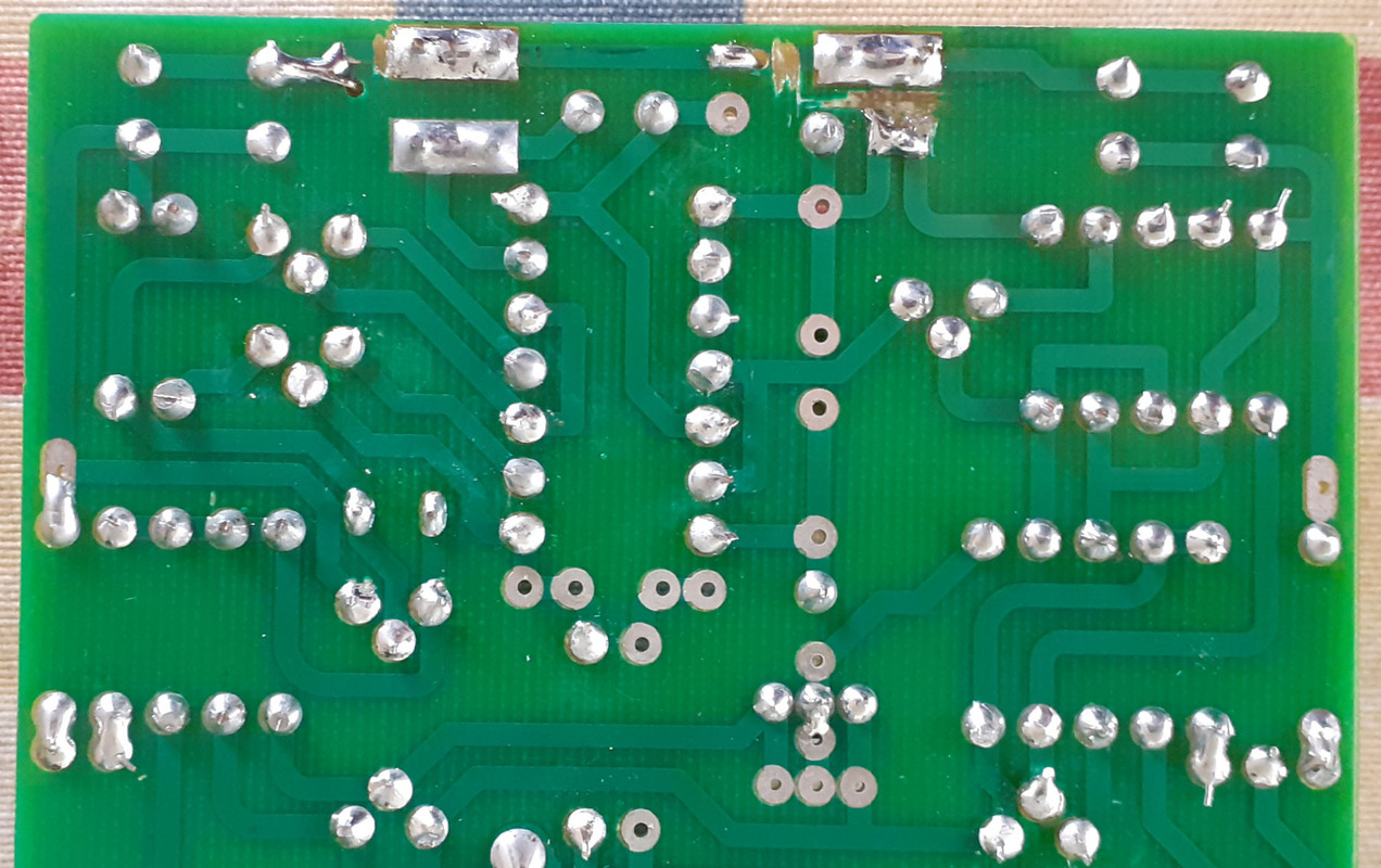
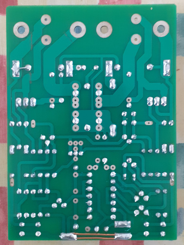
I have been reading the stuff on the Doug Self 'blameless' amp and inspired by this plus some other recent threads on here, I got the box of goodies out. In light of the Self stuff, it struck me that the earth arrangement at the input, with the incoming screen connection and the adjacent earth return to the psu being 30mm apart might be a source or ripple injection as the input loading and the F/B cap go to the psu return point and are thus not common with the incoming screen. I decided to measure the resistance of this trace out of curiosity by using my bench psu and a dummy load of 2x15R // to give 7R5. Adjusting the psu to give 7.5Vdc across the dummy load gives 1A current and passing that through these two connections and the trace, with my DVM clipped to the board so it makes contact with the solder pads beneath showed 14.7mVdc ie roughly 15mR:
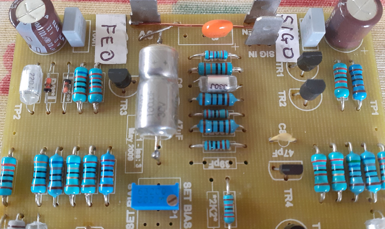
I then soldered a short 'u' shaped piece of wire to the back to bridge these two 'earth' points:
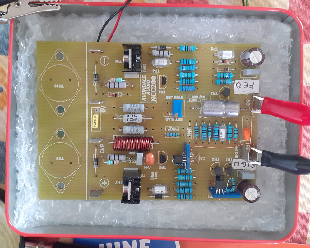
and then reconnected as before:
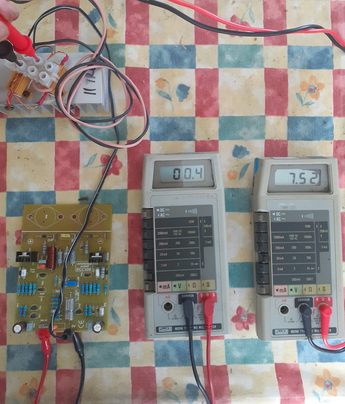
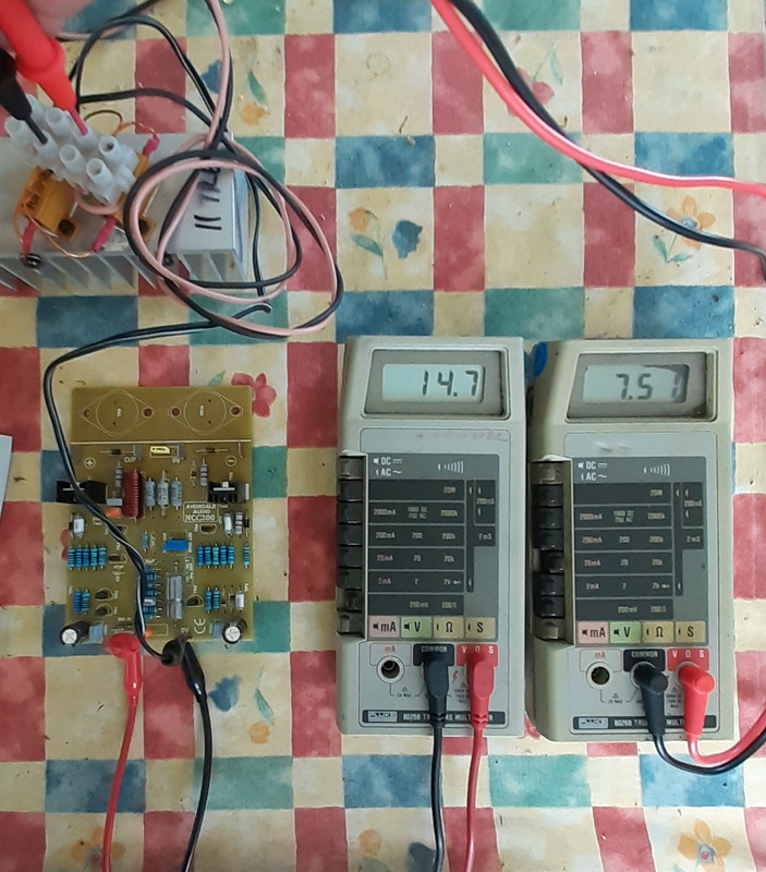
This now gives 0.4mVdc, equivalent to 0.4mR, which is a 30dB improvement! Thinking about this, at 100Hz a 100uF cap has an impedance of circa 15R. Therefore any ripple voltage across the capacitor will induce ripple between these two points at -60dB. The modification should now reduce that to approaching -90dB. The screen connection is at the +ve supply side compared the the psu return and this probably explains why the board responds well to regulation of the +ve supply as this removes any ripple between these two points.
I now have to decide how much of the 'blameless' circuit to incorporate... Initially I'm inclined to do the current mirror and the VAS mods on one board, then 'jiggle' the circuit boards so the drivers work as emitter-followers and feed it with my 3.1kHz low distortion signal source and scope the output.
I have been reading the stuff on the Doug Self 'blameless' amp and inspired by this plus some other recent threads on here, I got the box of goodies out. In light of the Self stuff, it struck me that the earth arrangement at the input, with the incoming screen connection and the adjacent earth return to the psu being 30mm apart might be a source or ripple injection as the input loading and the F/B cap go to the psu return point and are thus not common with the incoming screen. I decided to measure the resistance of this trace out of curiosity by using my bench psu and a dummy load of 2x15R // to give 7R5. Adjusting the psu to give 7.5Vdc across the dummy load gives 1A current and passing that through these two connections and the trace, with my DVM clipped to the board so it makes contact with the solder pads beneath showed 14.7mVdc ie roughly 15mR:
I then soldered a short 'u' shaped piece of wire to the back to bridge these two 'earth' points:
and then reconnected as before:
This now gives 0.4mVdc, equivalent to 0.4mR, which is a 30dB improvement! Thinking about this, at 100Hz a 100uF cap has an impedance of circa 15R. Therefore any ripple voltage across the capacitor will induce ripple between these two points at -60dB. The modification should now reduce that to approaching -90dB. The screen connection is at the +ve supply side compared the the psu return and this probably explains why the board responds well to regulation of the +ve supply as this removes any ripple between these two points.
I now have to decide how much of the 'blameless' circuit to incorporate... Initially I'm inclined to do the current mirror and the VAS mods on one board, then 'jiggle' the circuit boards so the drivers work as emitter-followers and feed it with my 3.1kHz low distortion signal source and scope the output.